 |
|
|
|
SP 5200XS Series
Quick Reference Guide
Jumper & Switch Settings
 |
 |
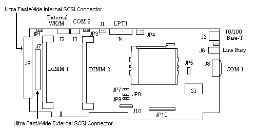
SP 5200XS Series Board Layout & End Bracket
Switch Settings
S1, Switch 1 and 2 - Supervisory Interrupt
The IES (Intelligent Environmental Sensor) module in the Density System communicates with the SP processors in the system via a hardware interrupt which is configurable as either IRQ 10 or IRQ 15. The interrupt is set with switch 1.
Note: The SP Series includes a secondary IDE controller for the Density System CD-ROM Drive. If this controller is enabled in the BIOS, it will use IRQ 15. If using the IES Supervisory System, its Interrupt must then be set to IRQ 10.
S1, Switch 3 - PS/2 Mouse IRQ
A PS/2 style mouse port is included on each SP processor. The mouse is connected to the SP board via the Density System multiplexer. If a mouse is not used, the port can be disabled to release the interrupt.
S1, Switch 4 - Not Used
Table 2-1, S1 Switch Settings
| Function | 1 |
2 |
3 |
4 |
| Supervisory Interrupt IRQ 10 | on |
off |
||
| Supervisory Interrupt IRQ 15 * | off |
on |
||
| No Supervisory Interrupt | off |
off |
||
| PS/2 Mouse on IRQ 12 * | on |
|||
| PS/2 Mouse on IRQ 12 Disabled | off |
|||
| *Factory
Settings (sw4 - not used) |
on | off | on |
Jumper Settings
The figure above shows the connector, switch and jumper locations on the board. Table 2-2 defines the jumper settings.
JP5 - Ethernet
The on-board DEC 21140 PCI Fast Ethernet (10/100 Mbps) controller can be disabled in the system BIOS and via hardware with jumper JP5.
JP3 - SCSI
The on-board Symbios 895 Ultra Fast/Wide SCSI controller can be enabled or disabled in the system BIOS and via hardware with jumper JP3.
Table 2-2, Jumpers
Jumper |
Function |
Jumper On Pins 1-2 |
Jumper On Pins 2-3 |
JP5 |
Ethernet |
Enabled |
Disabled |
JP3 |
SCSI |
Enabled |
Disabled |
JP7, JP8, & JP9 - CPU Voltage And Speed (Do Not Change)
Memory Configuration & Management
All SP Series memory is provided in 168 pin, 72 bit standard 60ns buffered DIMMs. DIMMs do not need to be installed in pairs, and different sizes may be mixed on a SP. Table 4-1 shows the Memory map for the SP processor. Table 4-2 defines the boards I/O configuration.
Click here
for the DIMM Memory Configuration Table
Table 4-1, Memory Map
Memory Range |
Size |
Use |
| 00000-9FFFF | 640KB | Conventional Memory |
| A0000-AFFFF | 64KB | VGA Graphics Buffer |
| B0000-B7FFF | 32KB | MDA Text Buffer |
| B8000-BFFFF | 32KB | VGA/CGA Text Buffer |
| C0000-C7FFF | 32KB | VGA Bios |
| C8000-DFFFF | 96KB | Available |
| E0000-FFFFF | 127KB | System & PCI BIOS |
Table 4-2, I/O Map
| ISA Ports | Description |
| 0000-00FF | Various "AT" functions in ISP chip and keyboard controller |
| 01F0-01F7 | IDE hard drive interface |
| 02F8-02FF | COM2 |
| 03A0 | Cubix supervisory interface |
| 03A8-03AF | IES serial port |
| 03B4-03B5 | VGA |
| 03BC-03BF | LPT1 |
| 03C0-03CF | VGA |
| 03D4-03D5 | VGA |
| 03F0-03F7 | Floppy / IDE |
| 03F8-03FF | COM1 |
System Interrupts
The 16 system hardware interrupts on the SP are represented in Table 4 - 4. Interrupts are managed by two standard 8259A Programmable Interrupt Controllers (PICs). Interrupts at IRQ 0 through 7 are located on the main PIC; IRQ 8 through 15 are on the SLAVE PIC.
Table 4-3, System Interrupts
IRQ |
Description |
IRQ |
Description |
0 |
Timer clock | 8 |
Real Time Clock |
1 |
Keyboard | 9 |
Redirected IRQ 2 |
2 |
Second OIC controller | 10 |
Set By PCI Plug & Play at boot time |
3 |
COM2 | 11 |
Set By PCI Plug & Play at boot time |
4 |
COM1 | 12 |
Available (or PS/2 Mouse) |
5 |
Set By PCI Plug & Play at boot time | 13 |
Math Coprocessor |
6 |
Floppy Disk Controller | 14 |
Primary IDE Controller |
7 |
LPT1 | 15 |
Secondary IDE Controller (or IES) |
Systems | Circuit Boards | Other Products | Software | Hardware Identifier
Other Vendors | Technical Notes | Downloads | Search | Support Home Page
This document, and all
Web Site contents, Copyright ©
2000 by Cubix Corp., Carson City, NV, USA.