|
|
|
|
BC 5xxxTX Series
Quick Reference Guide
Switches & Jumpers
 |
|
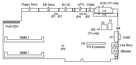
Figure 2-1, BC 5200TX Series Board Layout & End Bracket
Switch Settings
Figure 2-1 shows the switch locations. Table 2-1 and 2-2 define the settings for switch S1 and S2.S1, Switch 1 and 2 - Reset on Loss of DCD / DSR
The BC 5200TX can be configured to perform a hardware reset when the Data Carrier Detect (DCD) or Data Set Ready (DSR) signal changes from true to false on the COM1 serial port. This feature is designed for use in remote communication applications where the board is used to host dial in sessions through the COM 1 Port on a network, as it forces the BC to reset after each session. The reset causes the BC hardware to return to its initial state and also prevents the next dial in user from accessing data left in memory by the previous user. This function is available on COM1 only.
Table 2-1, S1 Switch Settings
Reset Condition |
1 2 |
|
| Reset when DSR drops on COM1 | on |
off |
| Reset when DCD drops on COM1 | off |
on |
| Reset when DCD or DSR drops on COM1 | on |
on |
| Reset Disabled * | off |
off |
*Factory Setting |
off |
off |
S2, Switch 1 and 2 - Supervisory Interrupt
The IES (Intelligent Environmental Sensor) module in the Density System communicates with the BC processors in the system via hardware interrupt IRQ 15. The interrupt is set with switch 1 and 2.S2, Switch 3 - PS/2 Mouse IRQ
A PS/2 style mouse port is included on each BC processor. The mouse is connected to the board via the Density System multiplexer. If a mouse is not used, the port can be disabled to release the interrupt. To disable the mouse, switch S1-3, and the system BIOS must be set.S2, Switch 4 and 5 - SCSI Termination (Model BC5200TX only)
Termination for the SCSI cable is enabled or disabled with a hardware switch on the board. SCSI termination should be enabled when the SCSI cable terminates at the BC processor or if the SCSI interface is not used. The Symbios 825A SCSI adapter can be enabled or disabled in the system BIOS and via hardware with jumper (JP6). See Chapter 3 for SCSI device termination and Installation.Table 2-2, S2 Switch Settings
| Function | 1 |
2 |
3 |
4 |
5 |
| Supervisory Interrupt IRQ 10 | on |
off |
|||
| Supervisory Interrupt IRQ 15 * | off |
on |
|||
| No Supervisory Interrupt | off |
off |
|||
| PS/2 Mouse on IRQ 12 * | on |
||||
| PS/2 Mouse on IRQ 12 Disabled | off |
||||
| SCSI Upper 8 Bit Terminator Enabled * | off |
||||
| SCSI Upper 8 Bit Terminator Disabled | on |
||||
| SCSI Lower 8 Bit Terminator Enabled * | off |
||||
| SCSI Lower 8 Bit Terminator Disabled | on |
||||
| *Factory Settings | off |
on |
on |
off |
off |
Jumper Settings
Figure 2-1 shows the jumper locations on the board. Table 2-3 defines the jumper settings.
JP1 & JP2 - Factory Set (Do not change)
JP4, JP5, JP6 & JP8
Jumper |
Function |
Jumper ON |
Jumper OFF |
JP4 |
Video (S3 TRIO64+ Chipset) | Enabled |
Disabled |
JP5 |
Ethernet (DEC 21140 Chipset) | Enabled |
Disabled |
JP6 |
SCSI (Symbios 825A Controller) | Enabled |
Disabled |
JP8 |
Flash | Write Enable |
Write Protect |
Note: The Ethernet and SCSI Controllers can also be disabled in system BIOS
Memory Configuration & Management
All BC 5200TX system memory is provided in 72-pin, 36-bit standard 60ns SIMMs. Two SIMMs must be installed, and both SIMMs must be of an identical size. SIMM Memory Configuration| SIMM 1 | SIMM 2 | Total Memory |
| 4 | 4 | 8 |
| 8 | 8 | 16 |
| 16 | 16 | 32 |
| 32 | 32 | 64 |
| 64 | 64 | 128 |
| 128 | 128 | 256 |
Table 4-1, Memory Map
Memory Range |
Size |
Use |
| 00000-9FFFF | 640KB | Conventional Memory |
| A0000-AFFFF | 64KB | VGA Graphics Buffer |
| B0000-B7FFF | 32KB | MDA Text Buffer |
| B8000-BFFFF | 32KB | VGA/CGA Text Buffer |
| C0000-C7FFF | 32KB | VGA Bios |
| C8000-DFFFF | 96KB | Available |
| E0000-FFFFF | 127KB | System & PCI BIOS |
Table 4-2, I/O Map
| ISA Ports | Description |
| 0000-00FF | Various "AT" functions in ISP chip and keyboard controller |
| 01F0-01F7 | IDE hard drive interface |
| 02F8-02FF | COM2 |
| 03A0 | Cubix supervisory interface |
| 03A8-03AF | IES serial port |
| 03B4-03B5 | VGA |
| 03BC-03BF | LPT1 |
| 03C0-03CF | VGA |
| 03D4-03D5 | VGA |
| 03F0-03F7 | Floppy / IDE |
| 03F8-03FF | COM1 |
System Interrupts
The 16 system hardware interrupts on the SP are represented in Table 4 - 4. Interrupts are managed by two standard 8259A Programmable Interrupt Controllers (PICs). Interrupts at IRQ 0 through 7 are located on the main PIC; IRQ 8 through 15 are on the SLAVE PIC. Table 4-3, System InterruptsIRQ |
Description |
IRQ |
Description |
0 |
Timer clock | 8 |
Real Time Clock |
1 |
Keyboard | 9 |
Redirected IRQ 2 |
2 |
Second OIC controller | 10 |
Set By PCI Plug & Play at boot time |
3 |
COM2 | 11 |
Set By PCI Plug & Play at boot time |
4 |
COM1 | 12 |
Available (or PS/2 Mouse) |
5 |
Set By PCI Plug & Play at boot time | 13 |
Math Coprocessor |
6 |
Floppy Disk Controller | 14 |
Primary IDE Controller |
7 |
LPT1 | 15 |
Secondary IDE Controller (or IES) |
Systems | Circuit Boards | Other Products | Software | Hardware Identifier
Other Vendors | Technical Notes | Downloads | Search | Support Home Page
This document, and all
Web Site contents, Copyright ©
2000 by Cubix Corp., Carson City, NV, USA.