|
|
|
|
DP 6200 Series
Quick Reference Guide
(For PowerSMP Systems)
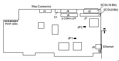
DP 6200 Series I/O Board
 |
|
S1, Switch 1 and 2 - Supervisory Interrupt
The IES module communicates with the DP processors in the subsystem via a hardware interrupt which is configurable as IRQ 10 or IRQ 15. Note that if the secondary IDE controller is used, IRQ 15 is not available. If no IES is installed, configure the DP for no IES Supervisory interrupt.S1, Switch 3, and 4 - SCSI Termination
Termination for the SCSI cable is enabled or disabled with a hardware switch on the board. SCSI termination should be enabled when the SCSI cable terminates at the DP processor or if the SCSI interface is not used. The Symbios 825A SCSI adapter can be enabled or disabled with hardware jumper JP2.See Chapter 3 for detailed SCSI termination information.
Table 2-1, I/O Board - S1 Switch Settings
| Function | 1 |
2 |
3 |
4 |
| Supervisory Interrupt IRQ 10 * | on |
off |
||
| Supervisory Interrupt IRQ 15 | off |
on |
||
| No Supervisory Interrupt | off |
off |
||
| Disable Lower 8 bit SCSI #1 Termination | on |
off |
||
| Disable Upper 8 bit SCSI #1 Termination | off |
on |
||
| Disable Lower 8 bit SCSI #2 Termination | off |
off |
||
| Disable Upper 8 bit SCSI #2 Termination | off |
off |
||
| *Factory Settings | on |
off |
off |
off |
Jumper Settings - I/O Board
Refer to figure 2-2 for jumper locations.JP1 - Ethernet Adapter
A DEC 21140 PCI Fast Ethernet (10/100 Mbps) controller is integrated onto the DP series I/O card. The controller can be disabled via jumper JP1 on the I/O card.JP2 - SCSI Adapters
Termination for the SCSI cable is enabled or disabled with a hardware switch on the board. SCSI termination should be enabled when the SCSI cable terminates at the DP processor or if the SCSI interface is not used. The Symbios 825A SCSI adapter can be enabled or disabled with hardware jumper JP2.Jumper |
Function |
Jumper 1-2 |
Jumper 2-3 |
JP1 |
Ethernet #2 (DEC 21140 Chipset) | Enabled |
Disabled |
JP2 |
SCSI #2 (Symbios 825A Controller) | Enabled |
Disabled |
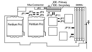
DP 6200 Series Processor Board
 |
|
Figure 2-2, DP 6200 Series Processor Board Layout & End Bracket
Jumper Settings - Processor Board
Refer to figure 2-1 for jumper locations.Table 2-3, Flash BIOS and Password Jumpers
Jumper |
Function |
Jumper ON |
Jumper OFF |
JP1 |
BIOS Password |
Normal |
Disabled |
JP13 |
Flash Reprogram |
Enabled |
Disabled |
Video
A hardware jumper (JP14) can be set on the processor board to disable the on-board S3 Trio64V+(765) video controller. If this controller is disabled, an external video controller with a video BIOS at address C0000 hexadecimal must be installed. Table 2-4, Video Enable/Disable JumperJumper |
Function |
Jumper Pins |
Jumper Pins |
JP14 |
S3 Video Enable |
1-2 |
2-3 |
Other Processor Board Jumpers
Jumpers 3 to 11 are processor dependent, and should not be changed from the factory settings.Memory Configuration & Management
All DP Series memory is provided in 168 pin, 72 bit standard 60ns buffered DIMMs. DIMMs do not need to be installed in pairs, and different sizes may be mixed on a SP. Table 4-1 shows the Memory map for the SP processor. Table 4-2 defines the boards I/O configuration.
Click here for the DIMM Memory Configuration Table
Table 4-1, Memory Map
Memory Range |
Size |
Use |
| 00000-9FFFF | 640KB | Conventional Memory |
| A0000-AFFFF | 64KB | VGA Graphics Buffer |
| B0000-B7FFF | 32KB | MDA Text Buffer |
| B8000-BFFFF | 32KB | VGA/CGA Text Buffer |
| C0000-C7FFF | 32KB | VGA Bios |
| C8000-DFFFF | 96KB | Available |
| E0000-FFFFF | 127KB | System & PCI BIOS |
Table 4-2, I/O Map
| ISA Ports | Description |
| 0000-00FF | Various "AT" functions in ISP chip and keyboard controller |
| 01F0-01F7 | IDE hard drive interface |
| 02F8-02FF | COM2 |
| 03A0 | Cubix supervisory interface |
| 03A8-03AF | IES serial port |
| 03B4-03B5 | VGA |
| 03BC-03BF | LPT1 |
| 03C0-03CF | VGA |
| 03D4-03D5 | VGA |
| 03F0-03F7 | Floppy / IDE |
| 03F8-03FF | COM1 |
System Interrupts
The 16 system hardware interrupts on the SP are represented in Table 4 - 4. Interrupts are managed by two standard 8259A Programmable Interrupt Controllers (PICs). Interrupts at IRQ 0 through 7 are located on the main PIC; IRQ 8 through 15 are on the SLAVE PIC.
Table 4-3, System InterruptsIRQ |
Description |
IRQ |
Description |
0 |
Timer clock | 8 |
Real Time Clock |
1 |
Keyboard | 9 |
Redirected IRQ 2 |
2 |
Second OIC controller | 10 |
Set By PCI Plug & Play at boot time |
3 |
COM2 | 11 |
Set By PCI Plug & Play at boot time |
4 |
COM1 | 12 |
Available (or PS/2 Mouse) |
5 |
Set By PCI Plug & Play at boot time | 13 |
Math Coprocessor |
6 |
Floppy Disk Controller | 14 |
Primary IDE Controller |
7 |
LPT1 | 15 |
Secondary IDE Controller (or IES) |
Systems | Circuit Boards | Other Products | Software | Hardware Identifier
Other Vendors | Technical Notes | Downloads | Search | Support Home Page
This document, and all
Web Site contents, Copyright ©
2000 by Cubix Corp., Carson City, NV, USA.