 |
|
|
|
BC 5xxxTE
Quick Reference Guide
 |
 |
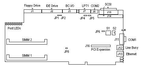
BC 5xxxTE Series Board Layout & End Bracket
This header requires a optional I/O adapter from Cubix. Attempting to connect a device directly to this connector will damage the board.
Note: The COM2 header requires a optional I/O adapter from Cubix. Attempting to connect a serial device directly to this connector will damage the board.
| JP1 - CPU Speed | factory set | Do not change |
| JP2 - CPU Speed | factory set | Do not change |
| JP4 - VGA | Enable = o-o o | Disable o o-o |
| JP5 - Ethernet | Enable = o-o o | Disable o o-o |
| JP6 - SCSI | Enable = o-o o | Disable o o-o |
| JP8 - Flash Write | On = Enabled | Off = Protect |
| SW1 | SW2 | |
| Reset when DSR drops on COM1 | ON | OFF |
| Reset when DCD drops on COM1 | OFF | ON |
| Reset when DCD or DSR drops on COM1 | ON | ON |
| Reset disabled | OFF | OFF |
| Factory settings (default) | OFF | OFF |
    Note: If positions 1 and 2 are both set to ON, then loss  of DSR or DCD will reset
     the BC processor.
| sw1 | SW2 | SW3 | SW4 | SW5 | |
| Supervisory IRQ to 10 | ON | OFF | |||
| Supervisory IRQ to 15 | OFF | ON | |||
| Disable Supervisory IRQ | OFF | OFF | |||
| PS/2 Mouse on IRQ 12 | ON | ||||
| Disable PS/2 Mouse | OFF | ||||
| SCSII Upper 8 Bit Terminator Enabled | OFF | ||||
| SCSI Upper 8 bit Terminator Disabled | ON | ||||
| SCSI Lower 8 Bit Terminator Enabled | OFF | ||||
| SCSI Lower 8 Bit Terminator Disabled | ON | ||||
| Factory settings (default) | OFF | ON | ON | OFF | ON |
All system memory is provided in 72-pin by 36 bit standard 70ns SIMM modules. For the proper placing of SIMM modules, see table below.
Note that both banks must be filled with the same type of SIMM. No empty banks are allowed.
| Simm Socket 1 | Simm Socket 2 | Total |
| 4 | 4 | 8 |
| 8 | 8 | 16 |
| 16 | 16 | 32 |
| 32 | 32 | 64 |
| 64 | 64 | 128 |
| 128 | 128 | 256 |
| IRQ | Description |
| 0 | Timer Click |
| 1 | Keyboard |
| 2 | Second PIC controller |
| 3 | COM2 |
| 4 | COM1 |
| 5 | Available/Ethernet |
| 6 | Floppy Disk Controller |
| 7 | LPT1 |
| 8 | Real-Time Clock |
| 9 | Redirected IRQ2 |
| 10 | Available/IES (s2) |
| 11 | Available/SCSI |
| 12 | Available/PS2 Mouse (s2) |
| 13 | Math Coprocessor |
| 14 | Fixed Disk Controller |
| 15 | Available/IES (s2) |
| 0000-00FF | Various "AT" functions |
| 01F0-01F7 | IDE hard drive interface |
| 02F8-02FF | COM 2 |
| 03A0 | Cubix supervisory interface |
| 03A8-03AF | IES serial port |
| 03B4-03B5 | VGA |
| 03BC-O3BF | LPT1 |
| 03C0-03CF | VGA |
| 03D4-03D5 | VGA |
| 03F0-03F7 | Floppy/IDE |
| 03F8-03FF | COM 1 |
| PCI PORTS | |
| 0CF8-0CFF | Used by PCI chipset |
| EC00-EC7F | Used by SCSI adapter |
| E880-E8FF | Used by Ethernet controller |
| 10000-7FFFF | 127MB | Extended Memory |
| E000-FFFF | 128KB | Reserved for system and PCI ROM BIOS |
| C800-DFFF | 96K | Available as Expanded (EMS) or Upper Memory (UMB) |
| C800-CABFF | 11K | SCSI BIOS (if installed) |
| B800-BFFF | 32K | VGA/CGA Video Memory |
| B000-B7FF | 32K | VGA/Mono Video Memory |
| A000-AFFF | 64K | VGA Video Memory |
| 0000-9FFF | 640K | Conventional DOS |
Systems | Circuit Boards | Other Products | Software | Hardware Identifier
Other Vendors | Technical Notes | Downloads | Search | Support Home Page
This document, and all
Web Site contents, Copyright ©
2000 by Cubix Corp., Carson City, NV, USA.