 |
|
|
|
CP 6xxx Series
Quick Reference Guide
Jumper & Switch Settings
 |
 |
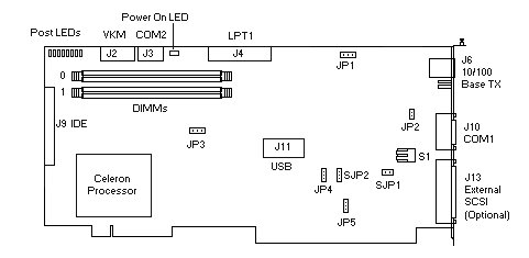
CP 6xxx Series Board Layout
& End Bracket
(Shown with optional External SCSI)
Switch 1 (S1) Settings
S1 - Position 1
The CP6xxx board comes equipped with a 2 position dip switch for reset control.
Position 1 is for data set ready (DSR). If position 1 is set in the "on"
position (the on and "off" positions are designated by an arrow clearly marked
on the switch), the CP6xxx board will reset the CPU on loss of data set ready. The factory
default setting for S1, position 1 is in the "off" position.
S1 - Position 2
S1, position 2 is for data carrier detect (DCD). If position 2 is set in the
"on" position, the CP6xxx board will reset the CPU when there is a loss of
carrier. The factory default setting for S1, position 2 is in the "on" position.
Table 1, S1 Switch Settings
| Function | 1 |
2 |
| Reset on Loss od DSR | on |
|
| Do Not Reset on Loss of DSR | off |
|
| Reset on Loss of DCD | on |
|
| Do Not Reset on Loss of DCD | off |
|
| Factory Default | off |
off |
Jumper Settings
The figure above shows the connector, switch and jumper locations on the board.
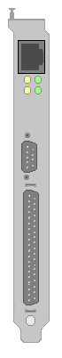
JP1 - Ethernet
The board is equipped wth an integrated Intel 82558 PCI fast Ethernet controller with an RJ-45 10/100 BASE TX connector on the mounting bracket at the rear of the board. The I/O addresses and interrupts are set by the PCI plug and play BIOS at boot time. The controller is enabled or disabled via jumper JP1 (see Figure above for JP1 location).
| Jumper | Function | Jumper On Pins 1-2 |
Jumper On Pins 2-3 |
| JP1 | Ethernet | Enabled | Disabled |
JP2 - CMOS Clear
The CMOS battery can be cleared by using JP2 (see Figure
above for JP2 location). This battery controls the maintenance and storage of three sets
of information: (1)the date and time generated and displayed on the computer screen;
(2)the peripheral setup, i.e. programming base register for the chip sets; and (3) the
password necessary for entry.
The first two sets of information can be changed during boot-up by following specific
directions displayed on the computer screen at the time the computer is booting-up. The
CMOS battery will automatically update and store the new information input. However, if
setup cannot be entered the normal way, CMOS clear is the recovery mechanism which can be
used. Or, if password information has been lost, the CMOS will need to be cleared so the
information can be updated, before program entry is possible.
To clear CMOS, the jumper must be removed from pins 1 and 2, and placed on pins 2 and 3.
After clearing, the jumper must be reinstalled on jumper pins 1 and 2 before updates can
be made.
| Jumper | Function | Jumper On Pins 1-2 |
Jumper On Pins 2-3 |
| JP2 | CMOS Clear | Normal | CMOS Clear |
JP3 - VGA
The on-board S3 video controller can
be enabled or disabled in the system BIOS and via hardware with jumper JP3.
| Jumper | Function | Jumper On Pins 1-2 |
Jumper On Pins 2-3 |
| JP3 | VGA | Enabled | Disabled |
JP4 - Flash Bios
If the Flash Bios is to be upgraded, a shunt mast be installed on the 2-pin jumper JP4 (see figure above for JP4 location). Upgrades typically come on a floppy disc and are accompanied by upgrade instructions. When the upgrade is complete, the shunt should be removed to protect the system from accidental erasure.
| Jumper | Function | Jumper On | Jumper Off |
| JP4 | Flash Write Enable | Enabled | Disabled |
JP5 - IES Interrupt (IRQ 10)
The IES module communicates with the CP6xxx processors in the
subsystem via a hardware interrupt which is IRQ 10. The supervisory interrupt is enabled
with JP5. If the CP6xxx board is part of the GlobalVision network, supervisory interrupt
is necessary and IES Interrupt must be enabled. If this board is not part of the
GlobalVision network, IES Interrupt can be disabled with JP5.
| Jumper | Function | Jumper On Pins 1-2 |
Jumper On Pins 2-3 |
| JP5 | IES Interrupt on IRQ 10 | Enabled | Disabled |
Symbios SCSI Controller Jumper Settings
The CP6xxxx board comes equipped to support an internal IDE
drive. However, for applications that require external SCSI devices, an integrated Wide
Ultra2 SCSI controller (Symbios 53C895) and an external SCSI cable connector (68-pin) can
be ordered as an option. This SCSI controller supports both LVD and Single-Ended SCSI
devices. The controller is enabled or disabled via a hardware jumper SJP2. (The "S'
proceding the "JP" designates the jumper is specific to SCSI functions.)
The SCSI controller is a bus master device which gains control of the PCI bus to transfer
data between the CPU memory and the SCSI devices. The I/O base address and interrupts are
set by the PCI plug and play BIOS at boot time.
If the SCSI controller is ordered, a SCSI configuration utility is available on boot-up of
the board. Shortly after the SCSI BIOS information displays, the configuration program can
be accessed by pressing "Control C". The configuration utility will allow you to
scan the SCSI bus, change configuration options and view a list of SCSI devices connected
to the board.
SJP2 - Enable/Disable SCSI Controller
As stated above, the on-board Symbios Wide Uttra2 SCSI controller can be enabled or
disabled with SJP2 (see Figure above for SJP2 location).
| Jumper | Function | Jumper On Pins 1-2 |
Jumper On Pins 2-3 |
| SJP2 | SCSI | Enabled | Disabled |
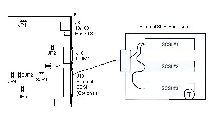
SJP1 - Enable/Disable SCSI Termination
The CP6xxx board comes from the factory with SCSI termination
enabled (i.e. a shunt is installed on SJP1, which is a 2-pin jumper). This allows the SCSI
connector to be configured as one end of the SCSI chain. If a situation requires the
disabling of the SCSI termination, the shunt simply needs to be removed from SJP1.
The SCSI controller supports up to 15 external SCSI hard drives, either Ultra2 LVD SCSI or
Single-Ended Wide SCSI devices. If Single-Ended Wide SCSI devices are used, the hard drive
at the end of the Single-Ended Wide SCSI chain must have its termination load enabled.
Consult the owners manual for the SCSI device for instructions on how to terminate. The
figure below demonstrates SCSI temination enabled on the CP6xxx board, and termination of
the eeternal SCSI device at the end of the SCSI chain.
Memory Configuration & Management
Table 4-1, Memory Map
Memory Range |
Size |
Use |
| 00000-9FFFF | 640KB | Conventional Memory |
| A0000-AFFFF | 64KB | VGA Graphics Buffer |
| B0000-B7FFF | 32KB | MDA Text Buffer |
| B8000-BFFFF | 32KB | VGA/CGA Text Buffer |
| C0000-C7FFF | 32KB | VGA Bios |
| C8000-DFFFF | 96KB | Available |
| E0000-FFFFF | 127KB | System & PCI BIOS |
Table 4-2, I/O Map
| ISA Ports | Description |
| 0000-00FF | Various "AT" functions in ISP chip and keyboard controller |
| 01F0-01F7 | IDE hard drive interface |
| 02F8-02FF | COM2 |
| 03A0 | Cubix supervisory interface |
| 03A8-03AF | IES serial port |
| 03B4-03B5 | VGA |
| 03BC-03BF | LPT1 |
| 03C0-03CF | VGA |
| 03D4-03D5 | VGA |
| 03F0-03F7 | Floppy / IDE |
| 03F8-03FF | COM1 |
System Interrupts
The 16 system hardware interrupts on the SP are represented in Table 4 - 4. Interrupts are managed by two standard 8259A Programmable Interrupt Controllers (PICs). Interrupts at IRQ 0 through 7 are located on the main PIC; IRQ 8 through 15 are on the SLAVE PIC.
Table 4-3, System Interrupts
IRQ |
Description |
IRQ |
Description |
0 |
Timer clock | 8 |
Real Time Clock |
1 |
Keyboard | 9 |
Redirected IRQ 2 |
2 |
Second OIC controller | 10 |
Set By PCI Plug & Play at boot time |
3 |
COM2 | 11 |
Set By PCI Plug & Play at boot time |
4 |
COM1 | 12 |
Available (or PS/2 Mouse) |
5 |
Set By PCI Plug & Play at boot time | 13 |
Math Coprocessor |
6 |
Floppy Disk Controller | 14 |
Not Used |
7 |
LPT1 | 15 |
Secondary IDE Controller (or IES) |
Systems | Circuit Boards | Other Products | Software | Hardware Identifier
Other Vendors | Technical Notes | Downloads | Search | Support Home Page
This document, and all
Web Site contents, Copyright ©
2000 by Cubix Corp., Carson City, NV, USA.