 |
|
|
|
SP 7400/7500 Series
Quick Reference Guide
Jumper & Switch Settings
 |
 |
Jumper Settings
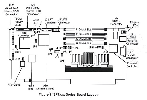
The figure above shows the connector, switch and jumper locations on the board.
JP1 - VGA
The on-board S3 video controller can be enabled or disabled in the system BIOS and via hardware with jumper JP1.
| Jumper | Function | Jumper On Pins 1-2 |
Jumper On Pins 2-3 |
| JP1 | VGA | Enabled | Disabled |
JP2 - Ethernet
The board is equipped wth an integrated Intel 82558 PCI fast
Ethernet controller with an RJ-45 10/100 BASE TX connector on the mounting bracket at the
rear of the board. The I/O addresses and interrupts are set by the PCI plug and play BIOS
at boot time. The controller is enabled or disabled via jumper JP2 (see Figure above for
JP2 location).
| Jumper | Function | Jumper On Pins 1-2 |
Jumper On Pins 2-3 |
| JP2 | Ethernet | Enabled | Disabled |
JP9 - Flash Bios
If the Flash Bios is to be upgraded, a shunt mast be
installed on the 2-pin jumper JP4 (see figure above for JP9 location). Upgrades typically
come on a floppy disc and are accompanied by upgrade instructions. When the upgrade is
complete, the shunt should be removed to protect the system from accidental erasure.
Other Jumpers
Jumpers JP4, 5, 6, 7 (CPU Speed) are processor dependent and should not be changed from factory setting. JP8 (Reduce Clock EMI) is factory set and should not be changed. JP3 is reserved for future use.
Symbios SCSI Controller Jumper Settings
The board is equipped with an integrated Wide Ultra2 SCSI
controller (Symbios 53C895). This SCSI controller supports both LVD and Single-Ended SCSI
devices*. The controller is enabled or disabled via a hardware jumper SJP2. (The "S'
proceding the "JP" designates the jumper is specific to SCSI functions.)
The SCSI controller is a bus master device which gains control of the PCI bus to transfer
data between the CPU memory and the SCSI devices. The I/O base address and interrupts are
set by the PCI plug and play BIOS at boot time.
If the SCSI controller is ordered, a SCSI configuration utility is available on boot-up of
the board. Shortly after the SCSI BIOS information displays, the configuration program can
be accessed by pressing "Control C". The configuration utility will allow you to
scan the SCSI bus, change configuration options and view a list of SCSI devices connected
to the board.
SJP2 - Enable/Disable SCSI Controller
As stated above, the on-board Symbios Wide Ultra2 SCSI controller can be enabled or
disabled with SJP2 (see Figure above for SJP2 location).
SJP1 - Enable/Disable SCSI Termination
The board comes from the factory with SCSI termination
enabled (i.e. a shunt is installed on SJP1, which is a 2-pin jumper). This allows the SCSI
connector to be configured as one end of the SCSI chain. If a situation requires the
disabling of the SCSI termination, the shunt simply needs to be removed from SJP1.
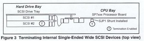
The SCSI controller supports either an Ultra2 LVD SCSI or Single-Ended Wide SCSI device.
The figure below shows termination for the Single-Ended Wide SCSI drive tray with
termination enabled on SCSI drive #2 and the SP 7xxx board.
If a LVD drive is in place, the Ultra2 LVD interface board on the drive tray supplies its own termination and all the Ultra2 LVD drives must therefore remain unterminated.
To disable on-board SCSI termination on the board for the purpose of adding external SCSI devices, the shunt must be removed from SPJ1 as shown below. The device on each end of the SCSI chain must be terminated. An end bracket with the external SCSI connector (68-pin) should be installed into an expansion slot adjacent to the SP Board for easy connection to the SCSI devices.
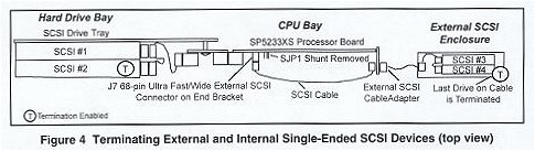
Table 4-1, Memory Map
Memory Range |
Size |
Use |
| 00000-9FFFF | 640KB | Conventional Memory |
| A0000-AFFFF | 64KB | VGA Graphics Buffer |
| B0000-B7FFF | 32KB | MDA Text Buffer |
| B8000-BFFFF | 32KB | VGA/CGA Text Buffer |
| C0000-C7FFF | 32KB | VGA Bios |
| C8000-DFFFF | 96KB | Available |
| E0000-FFFFF | 127KB | System & PCI BIOS |
Table 4-2, I/O Map
| ISA Ports | Description |
| 0000-00FF | Various "AT" functions in ISP chip and keyboard controller |
| 01F0-01F7 | IDE hard drive interface |
| 02F8-02FF | COM2 |
| 03A0 | Cubix supervisory interface |
| 03A8-03AF | IES serial port |
| 03B4-03B5 | VGA |
| 03BC-03BF | LPT1 |
| 03C0-03CF | VGA |
| 03D4-03D5 | VGA |
| 03F0-03F7 | Floppy / IDE |
| 03F8-03FF | COM1 |
System Interrupts
The 16 system hardware interrupts on the SP are represented in Table 4 - 4. Interrupts are managed by two standard 8259A Programmable Interrupt Controllers (PICs). Interrupts at IRQ 0 through 7 are located on the main PIC; IRQ 8 through 15 are on the SLAVE PIC.
Table 4-3, System Interrupts
IRQ |
Description |
IRQ |
Description |
0 |
Timer clock | 8 |
Real Time Clock |
1 |
Keyboard | 9 |
Redirected IRQ 2 |
2 |
Second OIC controller | 10 |
Set By PCI Plug & Play at boot time |
3 |
COM2 | 11 |
Set By PCI Plug & Play at boot time |
4 |
COM1 | 12 |
Available (or PS/2 Mouse) |
5 |
Set By PCI Plug & Play at boot time | 13 |
Math Coprocessor |
6 |
Floppy Disk Controller | 14 |
Primary IDE Controller |
7 |
LPT1 | 15 |
Secondary IDE Controller (or IES) |
Systems | Circuit Boards | Other Products | Software | Hardware Identifier
Other Vendors | Technical Notes | Downloads | Search | Support Home Page
This document, and all
Web Site contents, Copyright ©
2000 by Cubix Corp., Carson City, NV, USA.