 |
|
|
|
Chapter 3
BC4000 Hardware
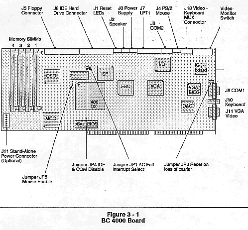
The Cubix BC 4000 board (Figure 3-1)is a 486DX-33 EISA-AT single-board computer for use in a passive backplane architecture. A BC 4000 board plugged into a passive backplane becomes a fully functional EISA-AT motherboard. This board meets the PCXI passive backplane specification for EISA systems.
Integrated onto the board are a floppy disk controller, IDE hard drive interface, COM1 port, COM2 header, LPT1 header, PS/2 mouse interface, and a VGA controller. The BC 4000 drives eight ISA slots and seven EISA slots. EISA bus master boards can reside in six of the EISA slots. As a special-order option, the board can have a standalone power input connector, so it can function as a standalone system without a backplane.
EISA Chip Set
A four-piece OPTI EISA chip set packaged in 160-pin QPFPs provides the following EISA-AT functions:
*8254 Timer
*8259 Compatible Programmable Interrupt Timers
*8257 Compatible DMA Controllers
*AT ISA/EISA BUS Controller
*Page Mode Memory Controller
*Memory Cache Controller
Clock
A battery-powered Dallas real time RAMified clock chip provides the time of day and date, standard CMOS RAM, and the 4K byte EISA configuration RAM.
Cache Memory
The BC 4000 board has a high-speed external cache memory array. The data portion uses four 32Kx8 20 ns memories yielding a 128K cache. The TAG RAM has a 32Kx9 15 ns memory and the DIRTY bit has an 8Kx8 15 ns memory. These chips are all static RAM memory. The TAG memory tracks the main-memory source of the data in cache, and the DIRTY bit indicates the validity of the data in a particular cache location.
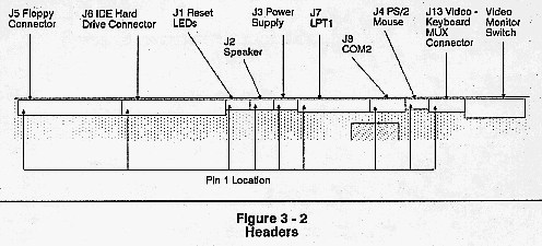
Figure 3-2 shows the board's headers, and the location of Pin 1 in each header.
Power Supply Status (J3) (Future Option)
The TL7705 voltage supervisory circuit determines when +5V has been stable long enough to let the CPU start. It also acts as a debounce circuit for the external reset switch.
Via connector J3 (Figure 3-2), the power supply can provide status of its AC input, batteries, and power quality. It also carries a signal from the BC 4000 to turn off the power supply. Loss of AC to the power supply can cause an interrupt to the BC 4000 (if selected by a jumper 1 on JP1). When this occurs, the BC 4000 monitors AC and battery status.
If low battery voltage status occurs before AC is restored, the BC 4000 turns off the power supply before the batteries can be damaged.
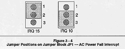
Jumper JP1 (Figure 3-4) selects the interrupt level for the AC Power Fail interrupt. The board supports interrupt levels 10, 15, or NONE. A jumper on pins 1-2 selects IRQ 15. A jumper on pins 2-3 selects IRQ 10. With no jumper installed, both interrupts are freed.
VGA Controller
The BC 4000 has an OAK Technologies OTI-067B VGA video controller.
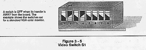
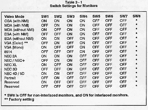
The OTI-066 DAC provides the VGA digital-to-analog conversion circuits. 512K bytes of 80ns video memory are available for the controller as VGA video memory. This allows a maximum resolution of 1024 X 768 pixels in 16 colors. The monitor must have <BI>analog<D> video inputs. Set Video Switch (S1) to match your monitor. Figure 3-5 shows Video Switch S1. Table 3-1 shows switch settings for each monitor.
I/O Ports (J7, J8, and J9)
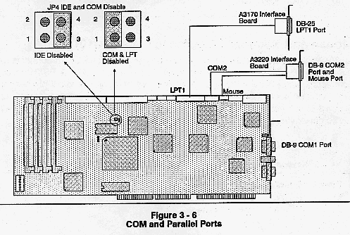
The BC 4000 board has a 16C552 integrated circuit with two COM ports and one LPT port. This chip has a 16-byte receive and transmit FIFO, which can be enabled by application software to enhance COM port performance. The COM1 port is wired to a DB-9 connector on the rear bracket of the board. The static and EMI filters for the signals on this port are on the BC 4000 board. The optional COM 2 port is on an A3220 Interface Board that connects to a 10-pin ribbon header. The interface board contains static and EMI filters and a DB-9 connector. The optional parallel port is on an A3170 Interface Board that connects to a 20-pin ribbon header. The interface board contains EMI filters and a DB-25 connector. To disable COM1, COM2, and LPT1 and to recover their interrupts and I/O addresses for use on the slot bus, install a jumper on JP4 pins 1-2 (Figure 3-6).
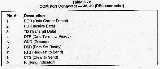
Table 3-2 shows the COM port connector J8, and J9.
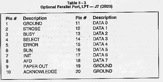
Table 3-3 shows the Optional LPT port, J7.
Mouse and Keyboard Interfaces (J4 and J10)
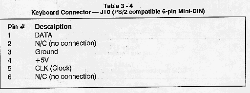
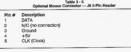
An 8042 chip controls a PS/2 keyboard and mouse. A PS/2 keyboard connects to a 6-pin mini-DIN connector (J10) mounted on the rear bracket. A PS/2 mouse connects to an optional A3220 Interface Board, which connects to a 5-pin header (J4) on the BC 4000 board. The Interface Board has a DB-9 mouse connector (see Figure 3-4). A jumper on jumper block JP5 enables the mouse port interrupt to IRQ 12. To disable the mouse port and recover IRQ 12, remove the jumper.
Table 3-4 shows the keyboard connector, J10.
Table 3-5 shows the optional Mouse connector, J8.
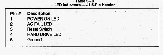
LED Indicators (J1)
Through J1, the board supports a remote reset switch and LED indicators that indicate POWER ON, AC FAIL, and HARD DRIVE ACTIVITY.
Table 3-6 shows the LED indicators 5 pin header, J1.
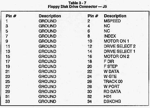
Floppy Disk Drive Controller (J5)
The floppy disk controller is a Western Digital 37C65B controller chip, which provides all the functions necessary for an AT-compatible floppy controller. It supports one or two AT-compatible 5 <$E1/4> or 3 <$E1/2> inch drives. The CMOS RAM must be configured with the correct types of drives connected for the drives to function correctly.
The floppy data cable must have the IBM twist in the cable between drives B and A.
Table 3-7 shows the Floppy disk drive connector, J5.
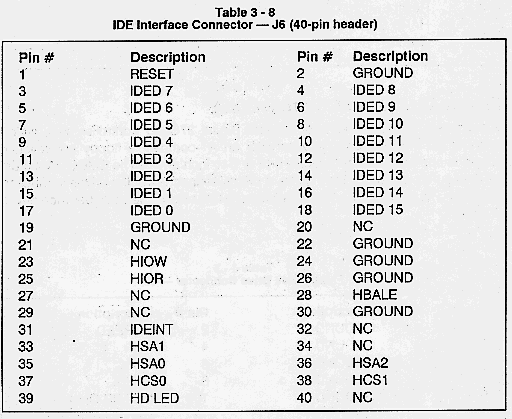
Hard Disk Drive Controller (J6)
The IDE hard drive interface connects an IDE-compatible hard drive to the BC 4000 board. Connector J6 is a 40 pin header that can be cabled directly to one or two IDE hard drives with a ribbon cable. If you use two drives, shunt them as drive 1 and drive 2. Configure the CMOS RAM with the proper drive types when you connect the IDE drives. To disable the IDE hard drive interface, install a jumper on JP4 pins 3-4 (see Figure 3-6). To free IRQ14, disconnect all drives from the 40 pin IDE connector.
Table 3-8 shows the IDE interface connector, J6.
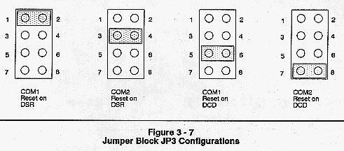
Hardware Reset (JP3)
You can configure the board to perform a hardware reset when the Carrier Detect or Data Set Ready signal on the COM connectors changes from true to false. Jumpers on jumper block JP3 determine the signal that resets each COM port. Figure 3-7 shows jumper block JP3 with a jumper in each position.
A jumper across pins 1 and 2 resets the hardware when the DSR signal drops on COM1.
A jumper across pins 3 and 4 resets the hardware when the DSR signal drops on COM2.
A jumper across pins 5 and 6 resets the hardware when the DCD signal drops on COM1.
A jumper across pins 7 and 8 resets the hardware when the DCD signal drops on COM2.
If you do not want a signal to reset the board, remove all the jumpers.
You can put only two jumpers on the jumper block. Do not put jumpers simultaneously on pins 1, 2, 3, and 4. Do not put jumpers simultaneously on pins 5, 6, 7, and 8.
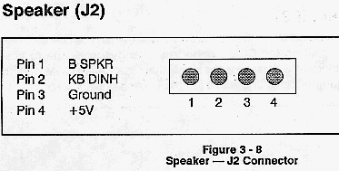
Speaker (J2)Figure 3-8
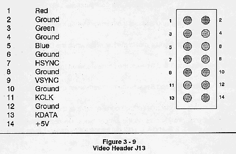
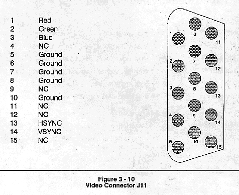
Video Ports (J12 and J13)Figure 3-9, and Figure 3-10
Memory Map
00000-9FFFF - System DRAM
A0000-BFFFF - VGA Video RAM
C0000-C7FFF - VGA video BIOS, may be shadowed
C8000-EFFFF - May be used as shadow RAM or R/W RAM
F0000-FFFFF - System BIOS, May be shadowed
100000-3FFFFFF - Extended RAM, to 64MB with 16MB SIMMS
0000-00FF - Various AT Functions in ISP Chip and keyboard controller
01F0-01FF - IDE hard drive interface
02F8-02FF - COM2
03A0 - Power supply status port
03B4-03B5 - VGA
03BC-03BF - LPT1
03C0-03CF - VGA
03D4-03D5 - VGA
03F0-03F7 - Floppy and IDE
03F8-03FF - COM1
EISA Ports
0400-04FF - Used by integrated system peripheral controller, (82C686) not all are used.
0800-08FF - Used by data bus controller (82C687)
0C00-0C08 - Used by data bus controller (82C687)
0C10-0C13 - Used by EISA bus controller (82C685)
0C20-0C22 - Used by integrated system peripheral controller, (82C686)
0C30-0C4F - Used by memory cache controller (82C682)
0C80-0C83 - Used by data bus controller (82C687) for EISA ID
NMI - Parity and VGA
0 - Timer
1 - Keyboard
2 - Expansion input for 8-15
3 - COM2 (may be disabled by JP4 1-2)
4 - COM1 (may be disabled by JP4 1-2)
5 - Not used
6 - Floppy
7 - LPT1 (may be disabled by JP4 1-2)
8 - Relative time clock
9 - Not used, redirected to IRQ2
10 - May be used by AC power fail from power supply
11 - Not used
12 - PS/2 mouse interrupt (remove JP5 to disable)
13 - Numeric co-processor interrupt
14 - IDE hard drive interrupt (not used if no IDE device)
15 - May be used by AC power fail from power supply
The only DMA channel used by the 4000 board is channel 2 for the floppy disk controller. This controller cannot be disabled.
This document, and all Web contents, Copyright © 1997
by Cubix Corp., Carson City, NV, USA.