 |
|
|
|
SP 5200 Series
Chapter 3 - Installation
SP Series Board Installation
Installation in a Cubix Density System
SCSI Device Installation
The board is equipped with an integrated fast/wide SCSI adapter. This adapter is enabled or disabled via the Chipset option of the BIOS Setup utility and via hardware with jumper JP3. The SCSI adapter is a bus master device which gains control of the PCI bus to transfer data between the CPU memory and the SCSI devices. The I/0 base address and interrupts are set by the PCI plug and play BIOS at boot time.A SCSI configuration utility is available on boot-up of the board. Shortly after the SCSI BIOS information displays, the configuration program can be accessed by pressing Control C. The configuration utility will allow you to scan the SCSI bus, change configuration options, and view a list of SCSI devices connected to the board.
Termination
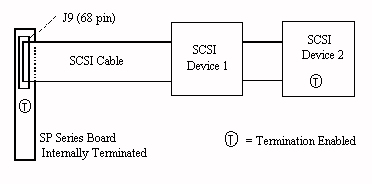
Figure 3-1, Terminating External SCSI Devices
SCSI termination is internally enabled on the board. The SCSI connector (J9) is configured as one end of the SCSI chain.
The last device on the SCSI cable must also supply a termination load to the cable. SCSI devices not at the end of the cable must have their termination loads disconnected.
Enabling and disabling a SCSI device's termination may involve a switch or shunt setting or the installation or removal of resistive SIP or DIP packages on their circuit board. Consult the installation manual for the SCSI device to determine its termination options.
Optional Peripheral Adapter Installation Optional Cubix peripheral adapter boards are available for VKM (Video/Keyboard/Mouse), LPT1, and COM 2. To install the adapters, follow the steps listed below. WARNING!MAKE SURE THE SYSTEM IS POWERED OFF AND
UNPLUGGED BEFORE BEGINNING THIS PROCEDURE.
Ethernet 10/100 Base-T Installation
The board is equipped with an integral DEC 21140 PCI fast Ethernet controller with a RJ-45 10/100 BASE-T connector (J5) on the mounting bracket at the rear of the board. This adapter is enabled or disabled via the "Chipset" option of the BIOS Setup utility and via hardware with jumper JP2. The I/O addresses and interrupts are set by the PCI plug and play BIOS at boot time. Software drivers are provided for this controller to support PC local area networks.Near the RJ-45 connector and visible in the mounting bracket are two sets of light emitting diodes (LED). On the lower set, the green LED will light when the interface has a valid connection to an Ethernet hub. The amber LED will light when the interface is set to 100 Mbit/s. On the upper set, the green LED indicates network activity, and the amber LED indicates a data collision on the network. These LEDs can be useful indicators of network activity.
Line Busy Installation
The Line Busy RJ-11 jack (J7) is designed to be connected to the phone line that attaches to a modem. Its purpose is the make the telephone line appear busy when the processor or modem is not ready to answer an incoming telephone call.The Line Busy circuit is inserted in parallel with the telephone line from the PBX to the modem. The Federal Communications Commission (FCC) has registered this circuit for use on PBX systems only and not for direct connection to the Public Telephone Network.
The Line Busy circuit is designed to be used on rotary PBX systems to keep incoming calls from ringing on lines that will not answer. The circuit uses Data Terminal Ready (DTR) from the Cubix processor's communication port to determine whether the processor is ready for a call. If DTR is false, the circuit creates an off-hook condition on the telephone line to force the rotary PBX to bypass this extension for an incoming call. When DTR is true, the Line Busy Circuit will terminate the off-hook condition, and the processor will respond to an incoming call. The Line Busy circuit on the SP is controlled by the COM1 DTR signal. The COM2 port has no effect on Line Busy. Cubix processors assert DTR false on the reset operation. It is the responsibility of the communications application running in the processor to assert the DTR signal true.
WARNING!The line busy circuit integrated onto the BC (J12) has been registered with the Federal Communications Commission for use on PBX's in the United States only. Use of this function outside the United States may violate local regulations and is not recommended by Cubix Corporation.
The line busy circuit complies with Part 68, FCC Rules.
FCC REGISTRATION NUMBER
2HEUSA-73508-KX-N
RINGER EQUIVALENCE O.O.B.
Line Busy Installation
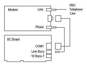
Figure 3-2, Line Busy Hook-up with Modem Phone Jack
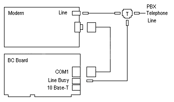
Figure 3-2, Line Busy Hook-up with Modem Phone Jack
Software Installation
Overview
To fully utilize all of the features integrated into the SP Series processors, the following software drivers and utilities are available on diskette, or can be obtained from the Cubix Customer Service Web site at: http://www.cubix.com/support
This document, and all Web contents, Copyright © 2000 by Cubix Corp., Carson City, NV, USA.