 |
|
|
|
BC Triton
Series
Chapter 4 - Technical Reference
BIOS
An American Megatrends, Inc. (AMI) system BIOS with embedded setup and hard disk setup utilities resides in Flash ROM on the board.
POST Display
The BC has eight LEDs arranged in two groups of four. As the system proceeds through its Power On System Test (POST) these LEDs display binary codes which can be used to diagnose board failures. The post codes are listed in Appendix A.
Memory Configuration
Memory Management
Figure 4-1 shows the Memory map for the BC Triton processor. Table 4-1 defines the boards I/O configuration.
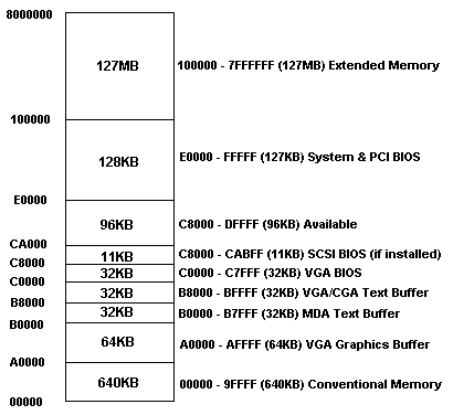
Figure 4-1, BC Triton Series Memory Map
| ISA Ports | Description |
| 0000-00FF | Various "AT" functions in ISP chip and keyboard controller |
| 01F0-01F7 | IDE hard drive interface |
| 02F8-02FF | COM2 |
| 03A0 | Cubix supervisory interface |
| 03A8-03AF | IES serial port |
| 03B4-03B5 | VGA |
| 03BC-03BF | LPT1 |
| 03C0-03CF | VGA |
| 03D4-03D5 | VGA |
| 03F0-03F7 | Floppy / IDE |
| 03F8-03FF | COM1 |
| PCI Ports | Description |
| 0CF8-0CFF | Used by PCI chip set |
| E880-E8FF | Used by Ethernet controller |
| EC00-ECFF | Used by SCSI adapter |
Table 4-1, BC Triton Series I/O Map
Keyboard/Mouse Controller
The BC has a PS/2 compatible keyboard controller with the AMI keyboard BIOS. The keyboard controller uses IRQ 1 for its interrupts, and requires no DMA channel. The keyboard controller also supports a PS/2 compatible mouse which uses IRQ 12. Switch S2 is used to enable the PS/2 mouse interrupt on IRQ 12 (refer to Chapter 2 for switch settings).
IDE Hard Drive Interface
An IDE hard drive interface is included on the BC for applications that require a hard disk drive. IDE drives include an AT compatible disk controller. The IDE interface circuit on the Triton Engine will support one or two IDE drives, while the Triton Server will support 4 IDE devices. The primary hard disk controller uses IRQ 14 for its interrupt. The
secondary hard disk controller, which is only used on the Triton Server, will use IRQ 15 when it is enabled. When adding an IDE drive to the board, the BIOS will auto-detect the new drive on boot. If the correct drive is not detected, use the BIOS to specify the hard drive parameters.
Note 1: To recover IRQ 14, all IDE drives must be removed from the 40-pin header cable.
Note 2: The Triton Server (BC5xxxTS) includes a secondary IDE controller. If this is enabled, it will use IRQ 15. The Cubix Supervisory System Interrupt must be set to IRQ 10 if it is to be used.
Floppy Disk Controller
The BC contains a PC/AT compatible floppy disk controller that supports all PC/AT floppy disk configurations. It is configured for industry standard single-speed floppy disk drives, and supports up to two of any combination of 5.25 or 3.5 inch drives. The BIOS setup program must be configured for the proper drives. The floppy controller uses IRQ 6 for its interrupt and DRQ 2 for its DMA channel. ISA processors allow the floppy disk controller to be disabled in the Peripheral Management Setup section of the System BIOS CMOS setup program.
SCSI Adapter
The BC Triton Series is equipped with an integrated fast/wide SCSI adapter. This adapter is enabled or disabled via the Chipset option of the BIOS Setup utility. Refer to Chapter 3 for drive installation instructions.
The BC Triton Series SCSI adapter is a bus master device which gains control of the PCI bus to transfer data between the CPU memory and the SCSI devices. The I/0 base address is set by the PCI plug and play BIOS at boot time. The SCSI adapter uses interrupt 11. The adapter does not use a shared memory window with the CPU.
The BC Triton Series SCSI adapter has SCSI cable termination which is enabled or disabled by setting switch S2 as described in Chapter 2. Refer to the SCSI Device Installation section of Chapter 3 for further details on SCSI termination.
Serial and Parallel Ports
Two serial ports and a parallel port are available on the BC processor board. One serial port is accessible through a standard DB-9 connector on the rear bracket (J11). The other serial port (COM2) and the parallel port (LPT1) are accessible internally through header connectors (J8 and J7). All ports comply fully with PC/AT interrupt and I/0 port standards. External access to the internal I/0 connectors (COM2 and LPT1) is accomplished through Cubix-supplied adapter boards. Refer to the sections Optional LPT1 and Optional COM2 in Chapter 3 for more information.
Ethernet Controller
The BC is equipped with an integral DEC 21140 PCI fast Ethernet controller with a 10/100 BASE-T RJ-45 connector (J13) on the mounting bracket at the rear of the card. Software drivers are provided for this controller to support PC local area networks.
Near the RJ-45 connector and visible in the mounting bracket are two sets of light emitting diodes (LED). On the lower set, the green LED will light when the interface has a valid connection to an Ethernet hub. The amber LED will light when the interface is set to 100 Mbit/s. On the upper set, the green LED indicates network activity, and the amber LED indicates a data collision on the network. These LEDs can be useful indicators of network activity.
Ethernet Configuration
The BC Triton Series Ethernet adapter is a bus master device which gains control of the PCI bus to transfer data between the CPU and the network. This adapter is enabled or disabled via the "Chipset" option of the BIOS Setup utility. The I/O addresses are set by the PCI plug and play BIOS at boot time. The interrupt used by the Ethernet adapter is 5. Note that the BC Ethernet controller does not use a shared memory window on the CPU nor does it support diskless boot configurations.
Line Busy
Installed only on the BC Triton Engine (BC5xxxTE)
The Cubix Line Busy RJ-11 jack is designed to be connected to the phone line that attaches to a modem. Its purpose is the make the telephone line appear busy when the processor or modem is not ready to answer an incoming telephone call.
The Line Busy circuit is inserted in parallel with the telephone line from the PBX to the modem. The Federal Communications Commission (FCC) has registered this circuit for use on PBX systems only and not for direct connection to the Public Telephone Network.
The Line Busy circuit is designed to be used on rotary PBX systems to keep incoming calls from ringing on lines that will not answer. The circuit uses Data Terminal Ready (DTR) from the Cubix processor's communication port to determine whether the processor is ready for a call. If DTR is false, the circuit creates an off-hook condition on the telephone line to force the rotary PBX to bypass this extension for an incoming call. When DTR is true, the Line Busy Circuit will terminate the off-hook condition, and the processor will respond to an incoming call. The Line Busy circuit on the BC is controlled by the COM1 DTR signal. The COM2 port has no effect on Line Busy.
Cubix processors assert DTR false on the reset operation. It is the responsibility of the communications application running in the processor to assert the DTR signal true.
WARNING!
The line busy circuit integrated onto the BC (J12) has been registered with the Federal Communications Commission for use on PBX's in the United States only. Use of this function outside the United States may violate local regulations and is not recommended by Cubix Corporation.
The line busy circuit complies with Part 68, FCC Rules.
FCC REGISTRATION NUMBER
2HEUSA-73508-KX-N
RINGER EQUIVALENCE O.O.B.
Line Busy Installation
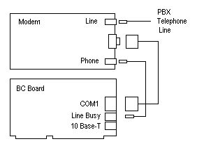
Figure 4-2
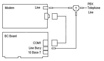
Figure 4-3
CMOS Battery
The BC has an internal battery that backs up the real time clock and CMOS memory. No external battery is required to retain date, time of day or setup information.
System Interrupts
The 16 system hardware interrupts on the BC are represented in Table 4 - 4. Interrupts are managed by two standard 8259A Programmable Interrupt Controllers (PICs). Interrupts at IRQ 0 through 7 are located on the main PIC; IRQ 8 through 15 are on the SLAVE PIC.
| IRQ | Description |
| 0 | Timer clock |
| 1 | Keyboard |
| 2 | Second PIC controller |
| 3 | COM2 |
| 4 | COM1 |
| 5 | Available OR Ethernet |
| 6 | Floppy Disk Controller |
| 7 | LPT1 |
| 8 | Real time clock |
| 9 | Redirected IRQ 2 |
| 10 | Available OR IES (S2) |
| 11 | Available OR SCSI |
| 12 | Available OR Mouse |
| 13 | Math Coprocessor |
| 14 | Primary Hard Disk controller |
| 15 | Available OR IES (S2) OR Secondary hard disk controller (TS only) |
Table 4-2, System Interrupts
This document, and all Web contents, Copyright © 1997 by Cubix Corp., Carson City, NV, USA.