 |
|
|
|
BC F Series
Chapter 4 - Technical Reference
BIOS
An American Megatrends, Inc. (AMI) system BIOS with embedded setup and hard disk setup utilities resides in EPROM on the board. At boot time, the data can be transferred to shadow RAM. This provides increased system performance, since RAM access is faster than EPROM access.
POST Display
The BC has eight LEDs arranged in two groups of four (refer to the illustrations in the Board Identification section of Chapter 1 for LED location). As the system proceeds through its Power On System Test (POST) these LEDs display binary codes which can be used to diagnose board failures. Refer to Appendix A for a description of these codes.
Memory - Hardware
All BC system memory is provided in 72-pin, 36-bit standard 70ns SIMM modules. These SIMMs are defined in Table 4-1.
Table 4 - 1
SIMM Definitions
| SIMM Type | Banks | Total Memory |
| 1M
x 36 2M x 36 4M x 36 8M x 36 16M x 36 |
Single Double Single Double Single |
4MB 8MB 16MB 32MB 64MB |
SIMM Configurations
BC 5133/5166/5200F/SE
| Simm Socket 1 | Simm Socket 2 | Total |
| 4 | 4 | 8 |
| 8 | 8 | 16 |
| 16 | 16 | 32 |
| 32 | 32 | 64 |
| 64 | 64 | 128 |
BC 5133/5166/5200F/SP
| 1 | 2 | 3 | 4 | 5 | 6 | Total |
| 4 | 4 | 8 | ||||
| 4 | 4 | 4 | 4 | 16 | ||
| 8 | 8 | 16 | ||||
| 4 | 4 | 4 | 4 | 4 | 4 | 24 |
| 8 | 8 | 4 | 4 | 24 | ||
| 8 | 8 | 4 | 4 | 4 | 4 | 32 |
| 8 | 8 | 8 | 8 | 32 | ||
| 16 | 16 | 32 | ||||
| 8 | 8 | 8 | 8 | 4 | 4 | 40 |
| 16 | 16 | 4 | 4 | 40 | ||
| 8 | 8 | 8 | 8 | 8 | 8 | 48 |
| 16 | 16 | 4 | 4 | 4 | 4 | 48 |
| 16 | 16 | 8 | 8 | 48 | ||
| 16 | 16 | 8 | 8 | 8 | 8 | 64 |
| 16 | 16 | 16 | 16 | 64 | ||
| 32 | 32 | 64 | ||||
| 16 | 16 | 16 | 16 | 4 | 4 | 72 |
| 32 | 32 | 4 | 4 | 72 | ||
| 16 | 16 | 16 | 16 | 4 | 4 | 72 |
| 32 | 32 | 4 | 4 | 4 | 4 | 80 |
| 32 | 32 | 8 | 8 | 80 | ||
| 32 | 32 | 8 | 8 | 8 | 8 | 88 |
| 16 | 16 | 16 | 16 | 16 | 16 | 96 |
| 32 | 32 | 8 | 8 | 8 | 8 | 96 |
| 32 | 32 | 16 | 16 | 96 | ||
| 32 | 32 | 16 | 16 | 4 | 4 | 104 |
| 32 | 32 | 16 | 16 | 8 | 8 | 112 |
| 32 | 32 | 16 | 16 | 16 | 16 | 128 |
| 32 | 32 | 32 | 32 | 128 | ||
| 64 | 64 | 128 | ||||
| 32 | 32 | 32 | 32 | 4 | 4 | 136 |
| 64 | 64 | 4 | 4 | 136 | ||
| 32 | 32 | 32 | 32 | 8 | 8 | 144 |
| 64 | 64 | 4 | 4 | 4 | 4 | 144 |
| 64 | 64 | 8 | 8 | 144 | ||
| 64 | 64 | 8 | 8 | 4 | 4 | 152 |
| 32 | 32 | 32 | 32 | 16 | 16 | 160 |
| 64 | 64 | 8 | 8 | 8 | 8 | 160 |
| 64 | 64 | 16 | 16 | 160 | ||
| 64 | 64 | 16 | 16 | 4 | 4 | 168 |
| 64 | 64 | 16 | 16 | 8 | 8 | 176 |
| 32 | 32 | 32 | 32 | 32 | 32 | 192 |
| 64 | 64 | 16 | 16 | 16 | 16 | 192 |
| 64 | 64 | 32 | 32 | 192 | ||
| 64 | 64 | 32 | 32 | 4 | 4 | 200 |
| 64 | 64 | 32 | 32 | 8 | 8 | 208 |
| 64 | 64 | 32 | 32 | 16 | 16 | 224 |
| 64 | 64 | 32 | 32 | 32 | 32 | 256 |
| 64 | 64 | 64 | 64 | 256 | ||
| 64 | 64 | 64 | 64 | 4 | 4 | 264 |
| 64 | 64 | 64 | 64 | 8 | 8 | 272 |
| 64 | 64 | 64 | 64 | 16 | 16 | 288 |
| 64 | 64 | 64 | 64 | 32 | 32 | 320 |
| 64 | 64 | 64 | 64 | 64 | 64 | 384 |
Memory Management
Memory between 640 KBytes and 1 MByte not required by hardware memory windows or BIOS can be made available to the installed memory manager. By configuring these areas as EMS page frames or Upper Memory Blocks, they can be used for loading and executing application software such as TSRs (Terminate and Stay Resident programs) and network drivers.
Memory maps for each type of BC processor are illustrated in the following figures.
BC 5133/5166/5200F/SE Memory map
| 10000-7FFFF | 127MB | Extended Memory |
| E000-FFFF | 128KB | Reserved for system and PCI ROM BIOS |
| C800-DFFF | 96K | Available as Expanded (EMS) or Upper Memory (UMB) |
| C800-CABFF | 11K | SCSI BIOS (if installed) |
| B800-BFFF | 32K | VGA/CGA Video Memory |
| B000-B7FF | 32K | VGA/Mono Video Memory |
| A000-AFFF | 64K | VGA Video Memory |
| 0000-9FFF | 640K | Conventional DOS |
BC 5133/5166/5200F/SP Memory map
| 10000-17FFFF | 384MB | Extended Memory |
| E000-FFFF | 128KB | Reserved for system and PCI ROM BIOS |
| C800-DFFF | 96K | Available as Expanded (EMS) or Upper Memory (UMB) |
| C800-CABFF | 11K | SCSI BIOS (if installed) |
| B800-BFFF | 32K | VGA/CGA Video Memory |
| B000-B7FF | 32K | VGA/Mono Video Memory |
| A000-AFFF | 64K | VGA Video Memory |
| 0000-9FFF | 640K | Conventional DOS |
BC F Series I/O Map
| ISA Ports | Description |
| 0000-00FF | Various "AT" functions in ISP chip and keyboard controller |
| 01F0-01F7 | IDE hard drive interface |
| 02F8-02FF | COM2 |
| 03A0 | Cubix supervisory interface |
| 03A8-03AF | IES serial port |
| 03B4-03B5 | VGA |
| 03BC-03BF | LPT1 |
| 03C0-03CF | VGA |
| 03D4-03D5 | VGA |
| 03F0-03F7 | Floppy / IDE |
| 03F8-03FF | COM1 |
| PCI Ports | Description |
| 0CF8-0CFF | Used by PCI chip set |
| FF80-FF9F | Used by Ethernet controller |
| FC00-FC7F | Used by SCSI adapter |
Keyboard/Mouse Controller
The BC has a PS/2 compatible keyboard controller with the AMI keyboard BIOS. The keyboard controller uses IRQ 1 for its interrupts, and requires no DMA channel.
The keyboard controller also supports a PS/2 compatible mouse which uses IRQ 12. Switch S2 is used to enable the PS/2 mouse interrupt on IRQ 12 (refer to Chapter 2 for switch settings).
IDE Hard Drive Interface
An IDE hard drive interface is included on the BC for applications that require a hard disk drive. IDE drives include an AT compatible disk controller. The IDE interface circuit will support one or two IDE drives. The hard disk controller uses IRQ 14 for its interrupt. When adding an IDE drive to the board, use the AMI BIOS setup program to select the drive type. See the American Megatrends, Inc. BIOS Configuration Program User's Guide for information on selecting IDE drive types.
The BC CMOS must be configured to properly set up the IDE interface. In the Standard CMOS Setup section, hard disk types for C: and D: must be entered. If a disk is not present, select "Not Installed". This should be done, for example, if the only hard drive in the system is a SCSI drive. ISA processors also require that the IDE interface be "Enabled" in the Peripheral Management Setup section (if no disk is present set the IDE interface to "Disabled").
To recover IRQ 14, all IDE drives must be removed from the 40-pin header cable.
Floppy Disk Controller
The BC contains a PC/AT compatible floppy disk controller that supports all PC/AT floppy disk configurations. It is configured for industry standard single-speed floppy disk drives, and supports up to two of any combination of 5.25 or 3.5 inch drives. The BIOS setup program must be configured for the proper drives. The floppy controller uses IRQ 6 for its interrupt and DRQ 2 for its DMA channel. ISA processors allow the floppy disk controller to be disabled in the Peripheral Management Setup section of the System BIOS CMOS setup program (refer to the American Megatrends, Inc. BIOS Configuration Program User's Guide).
SCSI Adapter
The BC F Series is equipped with an integrated fast SCSI-2 adapter. This adapter is enabled or disabled via the Chipset option of the BIOS Setup utility. A 50-pin ribbon header (J14) is located near the end bracket for connection of up to seven SCSI devices either inside or outside of the subsystem enclosure. For devices outside of the subsystem, an adapter board is available from Cubix that mounts on an end bracket next to the BC F Series and converts the 50-pin ribbon cable to a high density 50-pin connector suitable for a standard SCSI-2 shielded cable (50-pin). Refer to Chapter 3 for installation instructions.
The BC F Series SCSI adapter is a bus master device which gains control of the PCI bus to transfer data between the CPU memory and the SCSI devices. The SCSI adapter uses 96 I/0 port addresses and one interrupt. The I/0 base address is set by the PCI plug and play BIOS at boot time. The interrupt level is 11.
The BC F Series SCSI adapter does not use a shared memory window with the CPU.
The BC F Series SCSI adapter has SCSI cable termination which is enabled or disabled by setting switch S2 as described in Chapter 2. SCSI termination should be enabled when the SCSI cable terminates at the BC for either internal or external devices. When both external and internal devices are used and the BC is not at one end of the cable, termination should be disabled. If the SCSI interface is not used termination should be enabled. The default setting for termination is enabled. Refer to the SCSI Device Installation section of Chapter 3 for further details on SCSI termination.
Serial and Parallel Ports
Two serial ports and a parallel port are available on the BC processor board. One serial port is accessible through a standard DB-9 connector on the rear bracket (J11). The other serial port (COM2) and the parallel port (LPT1) are accessible internally through header connectors (J8 and J7). All ports comply fully with PC/AT interrupt and I/0 port standards. External access to the internal I/0 connectors (COM2 and LPT1) is accomplished through Cubix-supplied adapter boards. Refer to the sections Optional LPTI and Optional COM2 and Mouse in Chapter 3 for more information. Contact the Cubix Sales department to order the serial or parallel port adapter product required to access the COM2 or LPT1 ports.
If the ports are being installed on an ISA BC product, use the Peripheral Management Setup section of the System BIOS CMOS setup program to configure the serial and parallel ports (refer to the American Megatrends, Inc. BIOS Configuration Program User's Guide).
Ethernet Controller
The BC is equipped with an integral Ethernet contoller with a 10/100 BASE-T RJ-11 connector (J13) on the mounting bracket at the rear of the card. Software drivers are provided for this controller to support PC local area networks.
Near the RJ-45 connector and visible in the mounting bracket are two sets of light emitting diodes (LED). On the lower set, the green LED will light when the interface has a valid connection to an Ethernet hub. The amber LED will light when the interface is set to 100 mbit/s. On the upper set, the green LED indicates network activity, and the amber LED indicates a data collision on the network. These LEDs can be useful indicators of network activity.
Ethernet Drivers
The BC Series 10/100 BASE-T Driver Diskette contains drivers for the following network operating systems:
The different drivers and associated software are stored in subdirectories on the diskette. The appendices of this manual include installation procedures for each network. These installation instructions are intended to provide examples to aid the installer. Procedures for installing the drivers for each particular network configuration vary.
Ethernet Configuration
The BC F Series Ethernet adapter is a bus master device which gains control of the PCI bus to transfer data between the CPU and the network. This adapter is enabled or disabled via the "Chipset" option of the BIOS Setup utility. The Ethernet adapter uses 32 I/O port addresses and one interrupt. The I/O addresses are set by the PCI plug and play BIOS at boot time. The interrupt level is 5. Note that the BC Ethernet controller does not use a shared memory window on the CPU nor does it support diskless boot configurations.
Line Busy
The Cubix Line Busy RJ-11 jack is designed to be connected to the phone line that attaches to a modem. Its purpose is the make the telephone line appear busy when the processor or modem is not ready to answer an incoming telephone call.
The Line Busy circuit is inserted in parallel with the telephone line from the PBX to the modem. The Federal Communications Commission (FCC) has registered this circuit for use on PBX systems only and not for direct connection to the Public Telephone Network.
The Line Busy circuit is designed to be used on rotary PBX systems to keep incoming calls from ringing on lines that will not answer. The circuit uses Data Terminal Ready (DTR) from the Cubix processor’s communication port to determine whether the processor is ready for a call. If DTR is false, the circuit creates an off-hook condition on the telephone line to force the rotary PBX to bypass this extension for an incoming call. When DTR is true, the Line Busy Circuit will terminate the off-hook condition, and the processor will respond to an incoming call. The Line Busy circuit on the BC is controlled by the COM1 DTR signal. The COM2 port has no effect on Line Busy.
Cubix processors assert DTR false on the reset operation. It is the responsibility of the communications application running in the processor to assert the DTR signal true.
Line Busy Installation
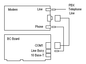
Figure 4-1
Line Busy Circuit Connected Via Modem Phone Jack
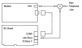
Figure 4-2
Line Busy Circuit Connected with "T" Jack
CMOS Battery
The BC has an internal battery that backs up the real time clock and CMOS memory. No external battery is required to retain date, time of day or setup information.
System Interrupts
The 16 system hardware interrupts on the BC are represented in Table 4 - 4. Interrupts are managed by two standard 8259A Programmable Interrupt Controllers (PICs). Interrupts at IRQ 0 through 7 are located on the main PIC; IRQ 8 through 15 are on the SLAVE PIC.
| IRQ | Description |
| 0 | Timer Click |
| 1 | Keyboard |
| 2 | Second PIC controller |
| 3 | COM2 |
| 4 | COM1 |
| 5 | Available/Ethernet |
| 6 | Floppy Disk Controller |
| 7 | LPT1 |
| 8 | Real-Time Clock |
| 9 | Redirected IRQ2 |
| 10 | Available/IES (s2) |
| 11 | Available/SCSI |
| 12 | Available/PS2 Mouse (s2) |
| 13 | Math Coprocessor |
| 14 | Fixed Disk Controller |
| 15 | Available/IES (s2) |
This document, and all Web contents, Copyright © 1997 by Cubix Corp., Carson City, NV, USA.