BC 5120/5150EP
Quick Reference Guide
Board Layout
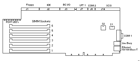
Connectors
| J1 |
Floppy Drive |
| J2 |
IDE Drive |
| J3 |
BC I/O |
| J7 |
LPT1 |
| J8 |
COM2 |
| J11 |
COM1 |
| J12 |
Line Busy |
| J13 |
Ethernet |
| J14 |
SCSI (8 bit) |
J1 - Floppy diskette
| 1 ground |
2 speed |
3 ground |
| 4 n/c |
5 ground |
6 n/c |
| 7 ground |
8 index |
9 ground |
| 10 motor on |
11 ground |
12 drive sel 2 |
| 13 ground |
14 motor sel 1 |
15 ground |
| 16 motor on 2 |
17 ground |
18 direction |
| 19 ground |
20 stop step |
21 ground |
| 22 write data |
23 ground |
24 write gate |
| 25 ground |
26 track 0 |
27 ground |
| 28 write protect |
29 ground |
30 read data |
| 31 ground |
32 side select |
33 ground |
| 34 disk change |
|
|
J2 - IDE Hard Disk
| 1 reset |
2 ground |
3 data 7 |
| 4 data 8 |
5 data 6 |
6 data 9 |
| 7 data 5 |
8 data 10 |
9 data 4 |
| 10 data 11 |
11 data 3 |
12 data 12 |
| 13 data 2 |
14 data 13 |
15 data 1 |
| 16 data 14 |
17 data 0 |
18 data 15 |
| 19 ground |
20 n/c |
21 n/c |
| 22 ground |
23 iow |
24 ground |
| 25 ior |
26 ground |
27 n/c |
| 28 bale |
29 n/c |
30 ground |
| 31 idint |
32 n/c |
33 sa1 |
| 34 n/c |
35 sa0 |
36 sa2 |
| 37 cs5 |
38 hcs1 |
39 n/c |
| 40 n/c |
|
|
J3 - BC I/O connector
| 1 gnd |
2 n/c |
3 ledsel- |
| 4 lanled |
5 ideled |
6 txdiled |
| 7 rxdiled |
8 n/c |
9 dtriled |
| 10 dcdiled |
11 spkr |
12 resetsw- |
| 13 ack |
14 poll |
15 mseclk |
| 16 mse data |
17 kclk |
18 kdata |
| 19 + 5vf |
20 vsync |
21 hsync |
| 22 gnd |
23 blu |
24 grn |
| 25 red |
26 gnd |
|
J7 - LPT1
This header requires a optional I/O adapter from Cubix. Attempting to
connect a device directly to this connector will damage the board.
J8 - COMM 2
| 1 DCD (data carrier detect) |
2 RD (receive data) |
| 3 TD (transmit data) |
4 DTR (data terminal ready) |
| 5 GND (ground) |
6 DSR (data set ready) |
| 7 RTS (request to send) |
8 CTS (clear to send) |
| 9 RI (ring indicator) |
|
Note: The COM2 header requires a optional I/O adapter from Cubix.
Attempting to connect a serial device directly to this connector will damage the board.
J11 - COMM 1
| 1 DCD (data carrier detect) |
2 RD (receive data) |
| 3 TD (transmit data) |
4 DTR (data terminal ready) |
| 5 GND (ground) |
6 DSR (data set ready) |
| 7 RTS (request to send) |
8 CTS (clear to send) |
| 9 RI (ring indicator) |
|
J12 - Line Busy (RJ11)
| 1 n/c |
2 n/c |
| 3 tip |
4 ring |
| 5 n/c |
6 n/c |
J13 - 10 Base-t Ethernet (RJ45)
| 1 transmit data (+) |
2 transmit data (-) |
| 3 Receive data (+) |
4 n/c |
| 5 n/c |
6 receive data (-) |
| 7 n/c |
8 n/c |
J14 - SCSI Interface
Information not available
Switches
Switch 1 - Reset on Loss of DCD or DSR
| |
sw1 |
sw2 |
| Reset when DSR drops on COM1 |
on |
off |
| Reset when DCD drops on COM1 |
off |
on |
| Reset when DCD or DSR drops on COM1 |
on |
on |
| Reset disabled |
off |
off |
| Factory settings (default) |
off |
off |
Note: If positions 1 and 2 are both set to ON, then loss
of DSR or DCD will reset the BC processor.
Switch 2 - Board Options and Interrupts
| |
sw1 |
sw2 |
sw3 |
sw4 |
sw5 |
| Supervisory IRQ to 10 |
on |
off |
|
|
|
| Supervisory IRQ to 15 |
off |
on |
|
|
|
| Disable Supervisory IRQ |
off |
off |
|
|
|
| PS/2 Mouse on IRQ 12 |
|
|
on |
|
|
| Disable PS/2 Mouse |
|
|
off |
|
|
| VGA Enabled |
|
|
|
|
on |
| VGA Disabled |
|
|
|
|
off |
| SCSI Terminator Enabled |
|
|
|
off |
|
| SCSI Terminator Disabled |
|
|
|
on |
|
| Factory settings (default) |
off |
on |
on |
off |
on |
SIMM's and Memory Map
Simm Module Configuration
All system memory is provided in 72-pin by 36 bit standard 70ns SIMM modules. For the
proper placing of SIMM modules, see table below.
| 1 |
2 |
3 |
4 |
5 |
6 |
Total |
| 4 |
4 |
|
|
|
|
8 |
| 4 |
4 |
4 |
4 |
|
|
16 |
| 8 |
8 |
|
|
|
|
16 |
| 4 |
4 |
4 |
4 |
4 |
4 |
24 |
| 8 |
8 |
4 |
4 |
|
|
24 |
| 8 |
8 |
4 |
4 |
4 |
4 |
32 |
| 8 |
8 |
8 |
8 |
|
|
32 |
| 16 |
16 |
|
|
|
|
32 |
| 8 |
8 |
8 |
8 |
4 |
4 |
40 |
| 16 |
16 |
4 |
4 |
|
|
40 |
| 8 |
8 |
8 |
8 |
8 |
8 |
48 |
| 16 |
16 |
4 |
4 |
4 |
4 |
48 |
| 16 |
16 |
8 |
8 |
|
|
48 |
| 16 |
16 |
8 |
8 |
8 |
8 |
64 |
| 16 |
16 |
16 |
16 |
|
|
64 |
| 32 |
32 |
|
|
|
|
64 |
| 16 |
16 |
16 |
16 |
4 |
4 |
72 |
| 32 |
32 |
4 |
4 |
|
|
72 |
| 16 |
16 |
16 |
16 |
4 |
4 |
72 |
| 32 |
32 |
4 |
4 |
4 |
4 |
80 |
| 32 |
32 |
8 |
8 |
|
|
80 |
| 32 |
32 |
8 |
8 |
8 |
8 |
88 |
| 16 |
16 |
16 |
16 |
16 |
16 |
96 |
| 32 |
32 |
8 |
8 |
8 |
8 |
96 |
| 32 |
32 |
16 |
16 |
|
|
96 |
| 32 |
32 |
16 |
16 |
4 |
4 |
104 |
| 32 |
32 |
16 |
16 |
8 |
8 |
112 |
| 32 |
32 |
16 |
16 |
16 |
16 |
128 |
| 32 |
32 |
32 |
32 |
|
|
128 |
| 64 |
64 |
|
|
|
|
128 |
| 32 |
32 |
32 |
32 |
4 |
4 |
136 |
| 64 |
64 |
4 |
4 |
|
|
136 |
| 32 |
32 |
32 |
32 |
8 |
8 |
144 |
| 64 |
64 |
4 |
4 |
4 |
4 |
144 |
| 64 |
64 |
8 |
8 |
|
|
144 |
| 64 |
64 |
8 |
8 |
4 |
4 |
152 |
| 32 |
32 |
32 |
32 |
16 |
16 |
160 |
| 64 |
64 |
8 |
8 |
8 |
8 |
160 |
| 64 |
64 |
16 |
16 |
|
|
160 |
| 64 |
64 |
16 |
16 |
4 |
4 |
168 |
| 64 |
64 |
16 |
16 |
8 |
8 |
176 |
| 32 |
32 |
32 |
32 |
32 |
32 |
192 |
| 64 |
64 |
16 |
16 |
16 |
16 |
192 |
| 64 |
64 |
32 |
32 |
|
|
192 |
| 64 |
64 |
32 |
32 |
4 |
4 |
200 |
| 64 |
64 |
32 |
32 |
8 |
8 |
208 |
| 64 |
64 |
32 |
32 |
16 |
16 |
224 |
| 64 |
64 |
32 |
32 |
32 |
32 |
256 |
| 64 |
64 |
64 |
64 |
|
|
256 |
| 64 |
64 |
64 |
64 |
4 |
4 |
264 |
| 64 |
64 |
64 |
64 |
8 |
8 |
272 |
| 64 |
64 |
64 |
64 |
16 |
16 |
288 |
| 64 |
64 |
64 |
64 |
32 |
32 |
320 |
| 64 |
64 |
64 |
64 |
64 |
64 |
384 |
IRQ Information
| IRQ |
Description |
| 0 |
Timer Click |
| 1 |
Keyboard |
| 2 |
Second PIC controller |
| 3 |
COM2 |
| 4 |
COM1 |
| 5 |
Available/Ethernet |
| 6 |
Floppy Disk Controller |
| 7 |
LPT1 |
| 8 |
Real-Time Clock |
| 9 |
Redirected IRQ2 |
| 10 |
Available/IES (s2) |
| 11 |
Available/SCSI |
| 12 |
Available/PS2 Mouse (s2) |
| 13 |
Math Coprocessor |
| 14 |
Fixed Disk Controller |
| 15 |
Available/IES (s2) |
I/O Map
| 0000-00FF |
Various "AT" functions |
| 01F0-01F7 |
IDE hard drive interface |
| 02F8-02FF |
COM 2 |
| 03A0 |
Cubix supervisory interface |
| 03A8-03AF |
IES serial port |
| 03B4-03B5 |
VGA |
| 03BC-O3BF |
LPT1 |
| 03C0-03CF |
VGA |
| 03D4-03D5 |
VGA |
| 03F0-03F7 |
Floppy/IDE |
| 03F8-03FF |
COM 1 |
| |
|
| PCI PORTS |
|
| 0CF8-0CFF |
Used by PCI chipset |
| FC00-FC7F |
Used by SCSI adapter |
| FF80-FF9F |
Used by Ethernet controller |
Memory Configuration
| 10000-7FFFF |
127MB |
Extended Memory |
| E000-FFFF |
128KB |
Reserved for system and PCI ROM BIOS |
| CAA00-DFFF |
96K |
Available as Expanded (EMS) or Upper Memory
(UMB) |
| C800-CABFF |
11K |
SCSI BIOS (if installed) |
| B800-BFFF |
32K |
VGA/CGA Video Memory |
| B000-B7FF |
32K |
VGA/Mono Video Memory |
| A000-AFFF |
64K |
VGA Video Memory |
| 0000-9FFF |
640K |
Conventional DOS |
This document, and all Web contents,
Copyright © 2000 by Cubix Corp., Carson City, NV, USA.
