 |
|
|
|
QL 4222
Quick Reference Guide
| 1 ground | 2 speed | 3 ground |
| 4 n/c | 5 ground | 6 n/c |
| 7 ground | 8 index | 9 ground |
| 10 motor on | 11 ground | 12 drive sel 2 |
| 13 ground | 14 motor sel 1 | 15 ground |
| 16 motor on 2 | 17 ground | 18 direction |
| 19 ground | 20 stop step | 21 ground |
| 22 write data | 23 ground | 24 write gate |
| 25 ground | 26 track 0 | 27 ground |
| 28 write protect | 29 ground | 30 read data |
| 31 ground | 32 side select | 33 ground |
| 34 disk change |
| 1 reset | 2 ground | 3 data 7 |
| 4 data 8 | 5 data 6 | 6 data 9 |
| 7 data 5 | 8 data 10 | 9 data 4 |
| 10 data 11 | 11 data 3 | 12 data 12 |
| 13 data 2 | 14 data 13 | 15 data 1 |
| 16 data 14 | 17 data 0 | 18 data 15 |
| 19 ground | 20 n/c | 21 n/c |
| 22 ground | 23 iow | 24 ground |
| 25 ior | 26 ground | 27 n/c |
| 28 bale | 29 n/c | 30 ground |
| 31 idint | 32 n/c | 33 sa1 |
| 34 n/c | 35 sa0 | 36 sa2 |
| 37 cs5 | 38 hcs1 | 39 n/c |
| 40 n/c |
| 1 gnd | 2 n/c | 3 ledsel- |
| 4 lanled | 5 ideled | 6 txdiled |
| 7 rxdiled | 8 n/c | 9 dtriled |
| 10 dcdiled | 11 spkr | 12 resetsw- |
| 13 ack | 14 poll | 15 mseclk |
| 16 mse data | 17 kclk | 18 kdata |
| 19 + 5vf | 20 vsync | 21 hsync |
| 22 gnd | 23 blu | 24 grn |
| 25 red | 26 gnd |
This header requires a optional I/O adapter from Cubix. Attempting to connect a device directly to this connector will damage the board.
| 1 DCD (data carrier detect) | 2 RD (receive data) |
| 3 TD (transmit data) | 4 DTR (data terminal ready) |
| 5 GND (ground) | 6 DSR (data set ready) |
| 7 RTS (request to send) | 8 CTS (clear to send) |
| 9 RI (ring indicator) |
Note: The COM2 header requires a optional I/O adapter from Cubix. Attempting to connect a serial device directly to this connector will damage the board.
| 1 DCD (data carrier detect) | 2 RD (receive data) |
| 3 TD (transmit data) | 4 DTR (data terminal ready) |
| 5 GND (ground) | 6 DSR (data set ready) |
| 7 RTS (request to send) | 8 CTS (clear to send) |
| 9 RI (ring indicator) |
| 1 n/c | 2 n/c |
| 3 tip | 4 ring |
| 5 n/c | 6 n/c |
Each QL 4222 board has a Mode Switch (DIP switch SW2). Positions 1 and 2 select the base I/O address used by the server driver to communicate with the QL 4000 processors. The QL interface requires eight consecutive I/O ports beginning with the base I/O address.
The I/O addresses selected must not be assigned to any non QL 4000 Series devices installed in the file server or bridge hosting the QL 4000 Series boards. However, all of the QL 4000 Series boards installed in this host should have the same base I/O address.
Reset on Loss of DCD or DSR
The QL 4222 is typically connected via the COM1 port to a modem performing remote communications over a telephone line. The COM1 port monitors the state of the Data Carrier Detect (DCD) or Data Set Ready (DSR) signals coming from the modem. The QL processors can be configured to perform an automatic hardware reset if DCD or DSR is dropped.
One practical usage of this feature is to force the QL processor to reset between remote sessions. This ensures users that they are connecting to a newly initialized system. It also verifies that users are properly disconnected from the network when their session terminates (i.e., a user will not remain logged into NetWare after "hanging up" the phone).
Depending upon the system configuration, either DCD or DSR will indicate that the telephone signal connection is established and that the modem is ready. Most configurations support DCD. However, if a multiplexer is installed between the QL 4222 COM1 port and the modem, it may be necessary to monitor DSR instead. Refer to the multiplexer manufacturer's documentation for this information.
The Mode Switch (DIP switch SW2) on the QL 4222 configures this feature.
| Function | 1 | 2 | 3 | 4 | 5 | 6 | 7 |
| * Select Base I/O Address 200 | on | on | on | ||||
| Select Base I/O Address 220 | on | off | on | ||||
| Select Base I/O Address 300 | off | on | on | ||||
| Select Base I/O Address 320 | off | off | on | ||||
| * Proc B: Disable reset Option | off | off | on | ||||
| Proc B: Reset on loss of DCD | off | on | on | ||||
| Proc B: Reset on loss of DSR | on | off | on | ||||
| Proc B: Reset on loss of DCD/DSR | on | on | on | ||||
| * Proc A: Disable reset Option | off | off | on | ||||
| Proc A: Reset on loss of DCD | off | on | on | ||||
| Proc A: Reset on loss of DSR | on | off | on | ||||
| Proc A: Reset on loss of DCD/DSR | on | on | on |
* = Factory Setting
Each node on a Novell network must be identified by a unique address. This address consists of two parts: a network number and a node number. When the Cubix server driver is installed, it must be assigned a unique network number. Each QL 4000 Series node to be supported by the server driver must be assigned a unique node number. The node number is selected by the I.D. Switch (DIP switch SW1) on the QL 4222 board. Valid node numbers range from 2 to 249. It is recommended that the QL 4222 node numbers be assigned consecutively beginning with node number 2 as this will maximize network performance.
| # | Switch SW1 | # | Switch SW1 | # | Switch SW1 |
| 002 | 7 off | 052 | 2,4,7 off | 0A2 | 1,3,7 |
| 004 | 6 | 054 | 2,4,6 | 0A4 | 1,3,6 |
| 006 | 6,7 | 056 | 2,4,6,7 | 0A6 | 1,3,6,7 |
| 008 | 5 | 058 | 2,4,5 | 0A8 | 1,3,5 |
| 00A | 5,7 | 05A | 2,4,5,7 | 0AA | 1,3,5,7 |
| 00C | 5,6 | 05C | 2,4,5,6 | 0AC | 1,3,5,6 |
| 00E | 5,6,7 | 05E | 2,4,5,6,7 | 0AE | 1,3,5,6,7 |
| 010 | 4 | 060 | 2,3 | 0B0 | 1,3,4 |
| 012 | 4,7 | 062 | 2,3,7 | 0B2 | 1,3,4,7 |
| 014 | 4,6 | 064 | 2,3,6 | 0B4 | 1,3,4,6 |
| 016 | 4,6,7 | 066 | 2,3,6,7 | 0B6 | 1,3,4,6,7 |
| 018 | 4,5 | 068 | 2,3,5 | 0B8 | 1,3,4,5 |
| 01A | 4,5,7 | 06A | 2,3,5,7 | 0BA | 1,3,4,5,7 |
| 01C | 4,5,6 | 06C | 2,3,5,6 | 0BC | 1,3,4,5,6 |
| 01E | 4,5,6,7 | 06E | 2,3,5,6,7 | 0BE | 1,3,4,5,6,7 |
| 020 | 3 | 070 | 2,3,4 | OCO | 1,2 |
| 022 | 3,7 | 072 | 2,3,4,7 | 0C2 | 1,2,7 |
| 024 | 3,6 | 074 | 2,3,4,6 | 0C4 | 1,2,6 |
| 026 | 3,6,7 | 076 | 2,3,4,6,7 | 0C6 | 1,2,6,7 |
| 028 | 3,5 | 078 | 2,3,4,5 | 0C8 | 1,2,5 |
| 02A | 3,5,7 | 07A | 2,3,4,5,7 | 0EC | 1,2,5,7 |
| 02C | 3,5,6 | 07C | 2,3,4,5,6 | 0CC | 1,2,5,6 |
| 02E | 3,5,6,7 | 07E | 2,3,4,5,6,7 | 0CE | 1,2,5,6,7 |
| 030 | 3,4 | 080 | 1 | 0D0 | 1,2,4 |
| 032 | 3,4,7 | 082 | 1,7 | 0D2 | 1,2,4,7 |
| 034 | 3,4,6 | 084 | 1,6 | 0D4 | 1,2,4,6 |
| 036 | 3,4,6,7 | 086 | 1,6,7 | 0D6 | 1,2,4,6,7 |
| 038 | 3,4,5 | 088 | 1,5 | OD8 | 1,2,4,5 |
| 03A | 3,4,5,7 | 08A | 1,5,7 | ODA | 1,2,4,5,7 |
| 03C | 3,4,5,6 | 08C | 1,5,6 | ODC | 1,2,4,5,6 |
| 03E | 3,4,5,6,7 | 08E | 1,5,6,7 | ODE | 1,2,4,5,6,7 |
| 040 | 2 | 090 | 1,4 | 0E0 | 1,2,3 |
| 042 | 2,7 | 092 | 1,4,7 | 0E2 | 1,2,3,7 |
| 044 | 2,6 | 094 | 1,4,6 | 0E4 | 1,2,3,6 |
| 046 | 2,6,7 | 096 | 1,4,6,7 | 0E6 | 1,2,3,6,7 |
| 048 | 2,5 | 098 | 1,4,5 | OE8 | 1,2,3,5 |
| 04A | 2,5,7 | 09A | 1,4,5,7 | OEA | 1,2,3,5,7 |
| 04C | 2,5,6 | 09C | 1,4,5,6 | OEC | 1,2,3,5,6 |
| 04E | 2,5,6,7 | 09E | 1,4,5,6,7 | OEE | 1,2,3,5,6,7 |
| 050 | 2,4 | 0A0 | 1,3 | OFO | 1,2,3,4 |
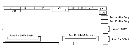
All QL 4222 system memory is provided in 72-pin by 36 bit standard 70ns SIMM modules in 4MB, 8MB, 16MB, 32MB or 64MB versions. There is one SIMM socket per processor. If double sided SIMM's are used, they must be TSOP (thin small outline package).
| 000 - 00F | DMA 1 |
| 020 - 021 | PIC 1 |
| 040 - 043 | Timer |
| 060, 064 8742 | Keyboard controller |
| 061 | Port B |
| 070 - 071 | CMOS RAM & NMI mask register |
| 080 | Manufacturing HEX display |
| 081 - 08F | DMA Page registers |
| 0A0 - 0A1 | PIC 2 |
| 0C0 - 0DF | DMA 2 |
| 1F0 - 1F7 | IDE Hard disk drive |
| 2F8 - 2FF | COM2 |
| 300 - 302 | QL Command/Status |
| 378 - 37F | LPT1 |
| 3B0 - 3DF | VGA |
| 3F0 - 3F7 | Floppy drive (QL 4222 only) |
| 3F8 - 3FF | COM1 |
| 46E8,102 | VGA configuration ports |
| NMI | Parity/VGA |
| 0 | Timer |
| 1 | Keyboard |
| 2 | Cascaded Input for PIC 2 |
| 3 | COM 2 |
| 4 | COM 1 |
| 5 | QL 3222: Interrupt from File Server QL 4222: Not Used |
| 6 | QL 3222: Interrupt from File Server QL 4222: Floppy Disk Drive |
| 7 | LPT 1 |
| 8 | Real Time Clock |
| 9 | VGA |
| 10 | Interrupt from File Server |
| 11 | Not Used |
| 12 | PS/2 Mouse Interrupt |
| 13 | Numeric Coprocessor Interrupt |
| 14 | IDE Hard Disk Drive |
| 15 | Not Used |
QL 3222
No DMA channels are used by the QL 3222.
QL 4222
DMA channel 2 is used by the floppy disk controller on the QL 4222.
| 00000 - 9FFFF | System Conventional Memory |
| A0000 - BFFFF | VGA Video memory |
| C0000 - C7FFF | VGA Video Bios copied to shadow RAM |
| C8000 - CBFFF | Diskless download code |
| CC000 - CFFFF | Server Interface |
| D0000 - EFFFF | Available |
| F0000 - FFFFF | AMI system BIOS copied to shadow RAM |
The areas of memory labeled as "Available" may be used by a memory manager to increase the amount of conventional memory available for applications.
The maps illustrated assumes a VGA or EGA configuration. If the application software to be run on the QL processor does not require VGA/EGA, additional memory becomes available as follows:
CGA: Uses B8000 to BFFFF - AOOOO to B7FFF is available.
Mono: Uses BOOOO to B7FFF - AOOOO to AFFFF & B8000 to BFFFF are available.
Be careful in assigning video memory for use by memory managers. If a VGA application is run on a QL processor which has reassigned video memory, that processor will fail.
This document, and all Web contents, Copyright © 1997 by Cubix Corp., Carson City, NV, USA.