BC 4035
Quick Reference Guide
Board Layout
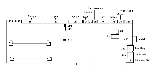
Connectors
J1 - Floppy diskette
| 1 ground |
2 speed |
3 ground |
| 4 n/c |
5 ground |
6 n/c |
| 7 ground |
8 index |
9 ground |
| 10 motor on |
11 ground |
12 drive sel 2 |
| 13 ground |
14 motor sel 1 |
15 ground |
| 16 motor on 2 |
17 ground |
18 direction |
| 19 ground |
20 stop step |
21 ground |
| 22 write data |
23 ground |
24 write gate |
| 25 ground |
26 track 0 |
27 ground |
| 28 write protect |
29 ground |
30 read data |
| 31 ground |
32 side select |
33 ground |
| 34 disk change |
|
|
J2 - IDE Hard Disk
| 1 reset |
2 ground |
3 data 7 |
| 4 data 8 |
5 data 6 |
6 data 9 |
| 7 data 5 |
8 data 10 |
9 data 4 |
| 10 data 11 |
11 data 3 |
12 data 12 |
| 13 data 2 |
14 data 13 |
15 data 1 |
| 16 data 14 |
17 data 0 |
18 data 15 |
| 19 ground |
20 n/c |
21 n/c |
| 22 ground |
23 iow |
24 ground |
| 25 ior |
26 ground |
27 n/c |
| 28 bale |
29 n/c |
30 ground |
| 31 idint |
32 n/c |
33 sa1 |
| 34 n/c |
35 sa0 |
36 sa2 |
| 37 cs5 |
38 hcs1 |
39 n/c |
| 40 n/c |
|
|
J3 - BC I/O
| 1 gnd |
2 n/c |
3 ledsel- |
| 4 lanled |
5 ideled |
6 txdiled |
| 7 rxdiled |
8 n/c |
9 dtriled |
| 10 dcdiled |
11 spkr |
12 resetsw- |
| 13 ack |
14 poll |
15 mseclk |
| 16 mse data |
17 kclk |
18 kdata |
| 19 + 5vf |
20 vsync |
21 hsync |
| 22 gnd |
23 blu |
24 grn |
| 25 red |
26 gnd |
|
J4 - Control Panel Connector
| 1 Resistor pull-up for Power on LED |
| 2 not used |
| 3 Reset switch (ground to reset computer) |
| 4 IDE Drive LED |
| 5 Ground |
J5 - Speaker Connector
| 1 Speaker data |
| 2 n/c |
| 3 Ground |
| 4 +5V (speaker power) |
J6 - Supervisory Port
| 1 ack (to supervisor) |
| 2 not used |
| 3 poll (from supervisor) |
| 4 not used |
J7 - LPT1
This header requires a optional I/O adapter from Cubix. Attempting to connect a device
directly to this connector will damage the board.
J8 - COM 2
| 1 DCD (data carrier detect) |
2 RD (receive data) |
| 3 TD (transmit data) |
4 DTR (data terminal ready) |
| 5 GND (ground) |
6 DSR (data set ready) |
| 7 RTS (request to send) |
8 CTS (clear to send) |
| 9 RI (ring indicator) |
|
Note: The COM2 header requires a optional I/O adapter from Cubix. Attempting to connect
a serial device directly to this connector will damage the board.
J9 - PS/2 Mouse Connector
This header requires a optional I/O adapter from Cubix. Attempting to connect a PS/2
mouse directly to this connector will damage the board.
J10 - Video/Kybd Mux Connector
 This header is for connection to the Optional Cubix Video
 Mux.
| 1 Red |
2 Ground |
| 3 Green |
4 Ground |
| 5 Blue |
6 Ground |
| 7 Hsync |
8 Ground |
| 9 Vsync |
10 mse data |
| 11 Kclk |
12 mse clk |
| 13 Kdata |
14 +5 (fused) |
J11 - COM 1
| 1 DCD (data carrier detect) |
2 RD (receive data) |
| 3 TD (transmit data) |
4 DTR (data terminal ready) |
| 5 GND (ground) |
6 DSR (data set ready) |
| 7 RTS (request to send) |
8 CTS (clear to send) |
| 9 RI (ring indicator) |
|
J12 - Line Busy
| 1 n/c |
2 n/c |
| 3 tip |
4 ring |
| 5 n/c |
6 n/c |
J13 - 10 Base-t Ethernet
| 1 transmit data (+) |
2 transmit data (-) |
| 3 Receive data (+) |
4 n/c |
| 5 n/c |
6 receive data (-) |
| 7 n/c |
8 n/c |
Switch & Jumper
Settings
Jumper JP1 & JP3 - CPU Speed
Factory configured - should not be changed.
| JP1- Pins 1-2 |
JP1- Pins 3 -4 |
JP3 |
CPU Speed |
| OFF |
ON |
1-2 |
SX-25, DX-25, DX2-50 |
| OFF |
OFF |
1-2 |
SX-33, DX-33, DX2-66, DX4-100 |
| ON |
OFF |
2-3 |
DX-40 (must have 40MHz chipset) |
Warning! P1 and JP3 are configured at the factory
for the CPU type installed and should not be changed
Jumper JP4 - Processor Type
| JP4 |
CPU
Type |
| OFF |
DX, DX2 |
| ON |
SX |
Warning! JP4 is configured at the factory for the CPU type installed and should not be
changed.
|
Switch 1 - Reset on Loss of DCD or DSR
| Reset
Condition |
Position |
| |
1 |
2 |
| Reset when DSR drops on COM1 |
ON |
OFF |
| Reset when DCD drops on COM1 |
OFF |
ON |
| Reset when DCD or DSR drops
on COM1 |
ON |
ON |
| *Reset Disabled |
OFF |
OFF |
| *Factory Setting |
OFF |
OFF |
| Note; If positions 1
and 2 are both set to ON, then loss of DSR will reset the BC 4035. |
Switch 2 - Board Options and Interrupts
| |
Position
|
| Function |
1 |
2 |
3 |
4 |
5 |
6 |
7 |
| *Enable Video Controller |
--- |
ON |
--- |
--- |
--- |
--- |
--- |
| Disable Video Controller |
--- |
OFF |
--- |
--- |
--- |
--- |
--- |
| Cubix Supervisory Interrupt
to IRQ 10 |
--- |
--- |
ON |
OFF |
--- |
--- |
--- |
| *Cubix Supervisory Interrupt
to IRQ 15 |
--- |
--- |
OFF |
ON |
--- |
--- |
--- |
| No Cubix Supervisory
Interrupt |
--- |
--- |
OFF |
OFF |
--- |
--- |
--- |
| *PS/2 Mouse Interrupt on IRQ
12 |
--- |
--- |
--- |
--- |
ON |
--- |
--- |
| PS/2 Mouse Interrupt on IRQ
12 Disabled |
--- |
--- |
--- |
--- |
OFF |
--- |
--- |
| Ethernet Interrupt on IRQ 3 |
ON |
--- |
--- |
--- |
--- |
ON |
OFF |
| *Ethernet Interrupt on IRQ 5 |
ON |
--- |
--- |
--- |
--- |
OFF |
ON |
| Disable Ethernet Controller |
OFF |
--- |
--- |
--- |
--- |
OFF |
OFF |
| *Factory Settings |
ON |
ON |
OFF |
ON |
ON |
OFF |
ON |
IRQ, I/O, SIMM's &
Memory Map
SIMM Definitions
| SIMM Type |
Banks |
Total Memory |
| 1M x 36 |
Single |
4MB |
| 2M x 36 |
Double |
8MB |
| 4M x 36 |
Single |
16MB |
| 8M x 36 |
Double |
32MB |
Simm Module Configuration
All BC 4030 system memory is provided in 72-pin by 36 bit standard 70ns SIMM modules in
4MB or 16MB versions. For the proper placing of SIMM modules, see table below.
| SIMM SOCKET 1 |
SIMM SOCKET 2 |
TOTAL MB |
| 4 |
|
4 |
| 8 |
|
8 |
| 8 |
4 |
12 |
| 8 |
8 |
16 |
| 16 |
|
16 |
| 32 |
|
32 |
| 32 |
4 |
36 |
| 32 |
8 |
40 |
| 32 |
16 |
48 |
| 32 |
32 |
64 |
IRQ Information
| IRQ |
Description |
| 0 |
Timer Clock |
| 1 |
Keyboard |
| 2 |
Second PIC controller |
| 3 |
COM2 / Ethernet (S2) |
| 4 |
COM1 |
| 5 |
Available / Ethernet (S2) |
| 6 |
Floppy disk controller |
| 7 |
LPT1 |
| 8 |
Real time clock |
| 9 |
Redirected IRQ 2 |
| 10 |
Available / IES (S2) |
| 11 |
Available / SCSI |
| 12 |
Available / Mouse (S2) |
| 13 |
Math coprocessor |
| 14 |
Hard disk controller |
| 15 |
Available / IES (S2) |
I/O Map
| ISA Ports |
Description |
| 0000 - 00FF |
Various "AT" functions in 499/82C206chip and
keyboard controller |
| 01F0 - 01FF |
IDE hard drive interface |
| 02F8 - 02FF |
COM2 |
| 0300 - 0317 |
Ethernet controller |
| 03A0 |
Cubix Supervisory System interface |
| 03B4 - 03B5 |
VGA |
| 03BC - 03BF |
LPT1 |
| 03C0 - 03CF |
VGA |
| 03D4 - 03D5 |
VGA |
| 03F0 - 03F7 |
Floppy / IDE |
| 03F8 - 03FF |
COM1 |
Memory Map
| F800-FFFF |
Reserved for AMI ROM BIOS. |
| F700-F7FF |
Available |
| F000-F6FF |
Reserved for AMI ROM BIOS |
| D000-EFFF |
Available as Expanded(EMS) or Upper Memory (UMB) |
| C800-CFFF |
Remote Boot EPROM if enabled.Otherwise available. |
| C000-C7FF |
Reserved for VGA BIOS |
| B800-BFFF |
VGA/CGA Video Memory |
| B000-B7FF |
VGA/Mono Video Memory |
| A000-AFFF |
VGA Video Memory |
| 0000-9FFF |
Conventional DOS |
This document, and all Web contents,
Copyright © 2000 by Cubix Corp., Carson City, NV, USA.
