 |
|
|
|
BC 4030
Quick Reference Guide
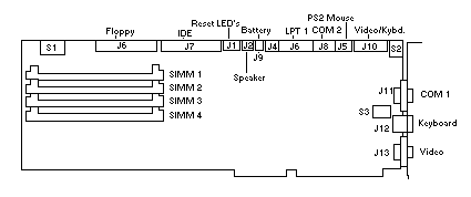
   1   ground           2   speed           3   ground
   4   n/c              5   ground          6   n/c
   7   ground           8   index           9   ground
   10  motor on 1       11  ground          12  drive sel 2
   13  ground           14  motor sel 1     15  ground
   16  motor on 2       17  ground          18  direction
   19  ground           20  stop step       21  ground
   22  write data       23  ground          24  write gate
   25  ground           26  track 0         27  ground
   28  write protect    29  ground          30  read data
   31  ground           32  side select     33  ground
   34  disk change
   1   reset            2   ground          3   data 7
   4   data 8           5   data 6          6   data 9
   7   data 5           8   data 10         9   data 4
   10  data 11          11  data 3          12  data 12
   13  data 2           14  data 13         15  data 1
   16  data 14          17  data 0          18  data 15
   19  ground           20  n/c             21  n/c
   22  ground           23  iow             24  ground
   25  ior              26  ground          27  n/c
   28  bale             29  n/c             30  ground
   31  idint            32  n/c             33  sa1
   34  n/c              35  sa0             36  sa2
   37  cs5              38  hcs1            39  n/c
   40  n/c
   1  Resistor pull-up for Power on LED
   2  ON Battery LED
   3  Reset switch (ground to reset computer)
   4  IDE Drive LED
   5  Ground
   1  Positive
   2  Negative
COMM 2 * DB9 connector from optional I/O Adapter.
   1  DCD  (data carrier detect)
   2  RD   (receive data)
   3  TD   (transmit data)
   4  DTR  (data terminal ready)
   5  GND  (ground)
   6  DSR  (data set ready)
   7  RTS  (request to send)
   8  CTS  (clear to send)
   9  RI   (ring indicator)

  Note: The COM2 header requires a optional I/O adapter from
        Cubix.  Attempting to connect a serial device
        directly
        to this connector will damage the board.
  This header requires a optional I/O adapter from Cubix.
  Attempting to connect a PS/2 mouse directly to this
  connector
  will damage the board.
  This header is for connection to the Optional Cubix Video
  Mux.

   1  Red               2  Ground
   3  Green             4  Ground
   5  Blue              6  Ground
   7  Hsync             8  Ground
   9  Vsync             10 Ground
   11 Kclk              12 Ground
   13 Kdata             14 +5 (fused)
   1  Data
   2  n/c
   3  Ground
   4  +5V
   5  Clock
   6  n/c
   1  Red             9  n/c
   2  Green           10 Ground
   3  Blue            11 n/c
   4  n/c             12 n/c
   5  Ground          13 Vsync
   6  Ground          14 Hsync
   7  Ground          15 n/c
   8  Ground
   This header requires a optional I/O adapter from Cubix.
   Attempting to connect a device directly to this connector
   will damage the board.
| sw1 | sw2 | sw3 | sw4 | sw5 | |
| Disable COM1, COM2, and LPT1 | - | on | - | - | - |
| Disable IDE hardware | on | - | - | - | - |
| *COM/LPT/IDE enabled | off | off | - | - | - |
| A.C. Fail on IRQ 10 | - | - | on | - | - |
| A.C. Fail on IRQ 15 | - | - | - | on | - |
| *No A.C. Fail IRQ used | - | - | off | off | - |
| Mouse port IRQ 12 enabled | - | - | - | - | on |
| *Mouse port IRQ 12 disabled | - | - | - | - | off |
* = default settings
| sw1 | sw2 | sw3 | sw4 | sw5 | |
| VGA (color) | off | on | off | on | * |
| VGA (mono) | on | off | off | on | * |
| 8514 | off | off | off | on | * |
| NEC 2A | on | on | on | off | * |
| NEC/NEC+ | off | on | on | off | * |
| NEC XL | no | off | on | off | * |
| NEC 3D | off | off | on | off | * |
| NEC 4D/5D | on | on | off | off | * |
                 SW 5 = OFF for non-interlaced monitors
                        ON  for interlaced monitors
| sw1 | sw2 | sw3 | sw4 | |
| Reset when DSR drops on COM1 | on | off | * | off |
| Reset when DSR drops on COM2 | off | on | off | * |
| Reset when DCD drops on COM1 | * | off | on | off |
| Reset when DCD drops on COM 2 | off | * | off | on |
* set to ON to monitor BOTH DCD and DSR. OFF if only the reset condition indicated is desired
  All BC 4030 system memory is provided in 72-pin by 36 bit
  stan
  dard 70ns SIMM modules in 4MB or 16MB versions. For the
  proper
  placing of SIMM modules, see table below.


 Simm Socket    1       2        3        4         Total MB

                4MB     NONE     NONE     NONE        4MB
                4MB     4MB      NONE     NONE        8MB
                4MB     4MB      4MB      NONE        12MB
                4MB     4MB      4MB      4MB         16MB
               16MB     NONE     NONE     NONE        16MB
               16MB     4MB      NONE     NONE        20MB
               16MB     4MB      4MB      NONE        24MB
               16MB     4MB      4MB      4MB         28MB
               16MB     16MB     NONE     NONE        32MB
               16MB     16MB     4MB      NONE        36MB
               16MB     16MB     4MB      4MB         40MB
               16MB     16MB     16MB     NONE        48MB
               16MB     16MB     16MB     4MB         52MB
               16MB     16MB     16MB     16MB        64MB
    IRQ        Description

     0         Timer Click
     1         Keyboard
     2         Second 8259A controller
     3         COM2
     4         COM1
     5         Available
     6         Floppy Disk Controller
     7         LPT1
     8         Real-Time Clock
     9         Redirected IRQ2
     10        Available
     11        Available
     12        Available
     13        Math Coprocessor
     14        Fixed Disk Controller
     15        Available
   FFFF /------------------/
        |                  |   F000-FFFF  Reserved for ROM
        BIOS.
        |                  |
        |     64K          |
        |                  |
        |                  |
   F000 |------------------|
        |                  |
        |    160K          |   C800-EFFF  Available for use
        as Expanded
        |                  |              (EMS) or Upper
        Memory (UMB).
        |                  |
        |                  |
        |                  |
        |                  |
        |                  |
   C800 |------------------|
        |     32K          |   C000-C7FF  Reserved for VGA
        BIOS
        |                  |
   C000 |------------------|
        |     32K          |   B800-BFFF  VGA/CGA Video
        Memory
        |                  |
   B800 |------------------|
        |     32K          |   B000-B7FF  VGA/Mono Video
        Memory
        |                  |
   B000 |------------------|
        |     64K          |   A000-AFFF  VGA Video Memory
        |                  |
   A000 |------------------|
        |                  |   0000-9FFF  Conventional DOS
        |    640K          |
        |                  |
        |                  |
        |                  |
        |                  |
   0000 /------------------/
This document, and all Web contents, Copyright © 2000 by Cubix Corp., Carson City, NV, USA.