|
|
|
|
QL 4001
Quick Reference Guide
This header requires a optional I/O adapter from Cubix. Attempting to connect a device directly to this connector will damage the board.
This header requires a optional I/O adapter from Cubix. Attempting to connect a device directly to this connector will damage the board.
| 1 ground | 2 speed | 3 ground |
| 4 n/c | 5 ground | 6 n/c |
| 7 ground | 8 index | 9 ground |
| 10 motor on | 11 ground | 12 drive sel 2 |
| 13 ground | 14 motor sel 1 | 15 ground |
| 16 motor on 2 | 17 ground | 18 direction |
| 19 ground | 20 stop step | 21 ground |
| 22 write data | 23 ground | 24 write gate |
| 25 ground | 26 track 0 | 27 ground |
| 28 write protect | 29 ground | 30 read data |
| 31 ground | 32 side select | 33 ground |
| 34 disk change |
Switch Settings
I/O Address
Each QL 4001 board has a seven position DIP switch (SW1).
Switches 1 and 2 of SW1 select the base I/O address used by the server driver to communicate with the QL 4001 processors. The QL interface requires 32 consecutive I/O ports beginning with the base I/O address. Base I/O address options are hexadecimal 200, 220, 300, and 320. The 32 port ranges are indicated below.
The I/O addresses selected must not be assigned to any non-QL 4000 Series devices installed in the file server or bridge hosting the QL 4000 boards. However, all of the QL 4000 Series boards installed in this host should have the same base I/O address.
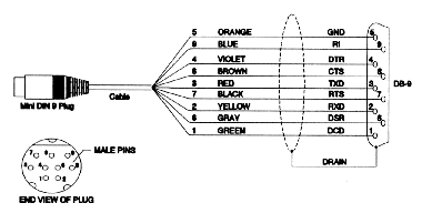
Reset on Loss of DCD/DCR
The QL 4001 is typically connected via a COM port to a modem to perform remote communications over a telephone line. The COM port monitors the state of the Data Carrier Detect (DCD) or Data Set Ready (DSR) signals coming from the modem. The QL processors can be configured to perform an automatic hardware reset if DCD or DSR is dropped.
One practical use of this feature is to force the QL processor to reset between remote sessions. This ensures users that they are connecting to a newly initialized system. It also verifies that users are properly disconnected from the network when their session terminates (i.e., a user will not remain logged into NetWare after "hanging up" the phone).
Depending upon the system configuration, either DCD or DSR will indicate that the telephone signal connection is established and that the modem is ready. Most configurations support DCD. However, if a multiplexer is installed between the QL 4001 COM port and the modem, it may be necessary to monitor DSR instead. Refer to the multiplexer manufacturer's documentation for this information.
The QL 4001 contains a seven position DIP switch (SW1 ) that configures this feature.
| Function | 1 | 2 | 3 | 4 | 5 | 6 | 7 |
| * Select Base I/O Address 200 | on | on | on | on | |||
| Select Base I/O Address 220 | on | off | on | on | |||
| Select Base I/O Address 300 | off | on | on | on | |||
| Select Base I/O Address 320 | off | off | on | on | |||
| * Monitor COM1 for DCD/DSR | on | on | on | ||||
| Monitor COM2 for DCD/DSR | on | on | off | ||||
| Monitor COM port for DSR | on | on | off | ||||
| * Monitor COM port for DCD | on | on | on | ||||
| Enable reset on loss of DCD/DSR | on | on | on | ||||
| * Disable reset on loss of DCD/DSR | on | on | off |
* = Factory Setting
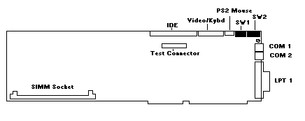
Each node on a Novell network must be identified by a unique address. This address consists of two parts: a network number and a node number. When the Cubix server driver is installed, it must be assigned a unique network number. Each QL 4000 series node to be supported by the server driver must be assigned a unique node number. The node number is selected by a DIP switch (SW2) on the QL 4000 board. Valid node numbers range from 1 to 250. It is recommended that the QL 4001 node numbers be assigned consecutively beginning with node number 1 as this will maximize network performance.
The QL 4001 board has an eight position DIP switch to identify the node number for each board. A switch is OFF when its handle is away from the board.
| 001 | 8 off | 030 | 3,4 off | 05F | 2,4,5,6,7,8 |
| 002 | 7 | 031 | 3,4,8 | 060 | 2,3 |
| 003 | 7,8 | 032 | 3,4,7 | 061 | 2,3,8 |
| 004 | 6 | 033 | 3,4,7,8 | 062 | 2,3,7 |
| 005 | 6,8 | 034 | 3,4,6 | 063 | 2,3,7,8 |
| 006 | 6,7 | 035 | 3,4,6,8 | 064 | 2,3,6 |
| 007 | 6,7,8 | 036 | 3,4,6,7 | 065 | 2,3,6,8 |
| 008 | 5 | 037 | 3,4,6,7,8 | 066 | 2,3,6,7 |
| 009 | 5,8 | 038 | 3,4,5 | 067 | 2,3,6,7,8 |
| 00A | 5,7 | 039 | 3,4,5,8 | 068 | 2,3,5 |
| 00B | 5,7,8 | 03A | 3,4,5,7 | 069 | 2,3,5,8 |
| 00C | 5,6 | 03B | 3,4,5,7,8 | 06A | 2,3,5,7 |
| 00D | 5,6,8 | 03C | 3,4,5,6 | 06B | 2,3,5,7,8 |
| 00E | 5,6,7 | 03D | 3,4,5,6,8 | 06C | 2,3,5,6 |
| 00F | 5,6,7,8 | 03E | 3,4,5,6,7 | 06D | 2,3,5,6,8 |
| 010 | 4 | 03F | 3,4,5,6,7,8 | 06E | 2,3,5,6,7 |
| 011 | 4,8 | 040 | 2 | 06F | 2,3,5,6,7,8 |
| 012 | 4,7 | 041 | 2,8 | 070 | 2,3,4 |
| 013 | 4,7,8 | 042 | 2,7 | 071 | 2,3,4,8 |
| 014 | 4,6 | 043 | 2,7,8 | 072 | 2,3,4,7 |
| 015 | 4,6,8 | 044 | 2,6 | 073 | 2,3,4,7,8 |
| 016 | 4,6,7 | 045 | 2,6,8 | 074 | 2,3,4,6 |
| 017 | 4,6,7,8 | 046 | 2,6,7 | 075 | 2,3,4,6,8 |
| 018 | 4,5 | 047 | 2,6,7,8 | 076 | 2,3,4,6,7 |
| 019 | 4,5,8 | 048 | 2,5 | 077 | 2,3,4,6,7,8 |
| 01A | 4,5,7 | 049 | 2,5,8 | 078 | 2,3,4,5 |
| 01B | 4,5,7,8 | 04A | 2,5,7 | 079 | 2,3,4,5,8 |
| 01C | 4,5,6 | 04B | 2,5,7,8 | 07A | 2,3,4,5,7 |
| 01D | 4,5,6,8 | 04C | 2,5,6 | 07B | 2,3,4,5,7,8 |
| 01E | 4,5,6,7 | 04D | 2,5,6,8 | 07C | 2,3,4,5,6 |
| 01F | 4,5,6,7,8 | 04E | 2,5,6,7 | 07D | 2,3,4,5,6,8 |
| 020 | 3 | 04F | 2,5,6,7,8 | 07E | 2,3,4,5,6,7 |
| 021 | 3,8 | 050 | 2,4 | 07F | 2,3,4,5,6,7,8 |
| 022 | 3,7 | 051 | 2,4,8 | 080 | 1 |
| 023 | 3,7,8 | 052 | 2,4,7 | 081 | 1,8 |
| 024 | 3,6 | 053 | 2,4,7,8 | 082 | 1,7 |
| 025 | 3,6,8 | 054 | 2,4,6 | 083 | 1,7,8 |
| 026 | 3,6,7 | 055 | 2,4,6,8 | 084 | 1,6 |
| 027 | 3,6,7,8 | 056 | 2,4,6,7 | 085 | 1,6,8 |
| 028 | 3,5 | 057 | 2,4,6,7,8 | 086 | 1,6,7 |
| 029 | 3,5,8 | 058 | 2,4,5 | 087 | 1,6,7,8 |
| 02A | 3,5,7 | 059 | 2,4,5,8 | 088 | 1,5 |
| 02B | 3,5,7,8 | 05A | 2,4,5,7 | 089 | 1,5,8 |
| 02C | 3,5,6 | 05B | 2,4,5,7,8 | 08A | 1,5,7 |
| 02D | 3,5,6,8 | 05C | 2,4,5,6 | 08B | 1,5,7,8 |
| 02E | 3,5,6,7 | 05D | 2,4,5,6,8 | 08C | 1,5,6 |
| 02F | 3,5,6,7,8 | 05E | 2,4,5,6,7 | 08D | 1,5,6,8 |
The QL 4001 is equipped with a minimum of 4 MB of RAM. The QL 4001 board's RAM resides in a standard PS/2 type 72-pin SIMM.
| 00000 - 9FFFF | System DRAM Memory |
| A0000 - BFFFF | VGA Video memory |
| C0000 - C7FFF | VGA Video BIOS copied to shadow RAM |
| C8000 - CBFFF | Reserved for diskless download code |
| CC000 - CFFFF | 16K dual-ported RAM |
| D0000 - EFFFF | Not used |
| F0000 - FFFFF | AMI System BIOS copied to shadow RAM |
| 000 - 00F | DMA 1 |
| 020 - 021 | PIC 1 |
| 040 - 043 | Timer |
| 060,064 | 8742 Keyboard Controller |
| 061 | Port B |
| 070 - 071 | CMOS RAM & NMI Mask Register |
| 080 | Manufacturing HEX Display |
| 081 - 08F | DMA Page Registers |
| 0A0 - 0A1 | PIC 2 |
| 0C0 - 0DF | DMA 2 |
| 1F0 - 1FF | IDE Hard Disk Drive |
| 2F8 - 2FF | COM 2 |
| 300 - 302 | QL 4001 Command/Status |
| 378 - 37F | LPT 1 |
| 3B0 - 3DF | VGA |
| 3F8 - 3FF | COM 1 |
| 46E8,102 | VGA Configuration Ports |
| NMI | Parity/VGA |
| 0 | Timer |
| 1 | Keyboard |
| 2 | Cascaded Input for PIC 2 |
| 3 | COM 2 |
| 4 | COM 1 |
| 5 | Not Used |
| 6 | Not Used |
| 7 | LPT 1 |
| 8 | Real Time Clock |
| 9 | VGA |
| 10 | Interrupt from Fileserver |
| 11 | Not Used |
| 12 | PS/2 Mouse Interrupt |
| 13 | Numeric Co-Processor Interrupt |
| 14 | IDE Hard Disk Drive |
| 15 | Not Used |
No DMA channels are used by the QL 4001.
This document, and all Web contents, Copyright © 1997 by Cubix Corp., Carson City, NV, USA.