 |
|
|
|
BC 4000
Chapter 3 - Technical Reference
System Components
System Interrupts
Switches, Connectors and Signals
EPROM BIOS
An American Megatrends, Inc. (AMI) system BIOS with embedded setup and hard disk setup utilities resides on the board (27C512 EPROM). At boot time, the data can be transferred to 32bit shadow RAM. This option provides increased system performance, since RAM access is more efficient than EPROM access. (Chapter 3 contains the AMI BIOS documentation.)
Video Controller
The BC 4000 contains an extended high resolution VGA graphics controller (Oak Technology OTI077). With 512K of video memory, this controller supports all standard VGA modes and the following extended modes: 640 x 480 with 256 colors; 800 x 600 with 256 colors; and 1024 x 768 with 16 colors. The connector on the board (J13) is an industry standard VGA connector (15pin highdensity DSubminiature).
Keyboard Controller
The BC 4000 has a PS/2 compatible keyboard controller (8042 or 8742) with the AMI keyboard BIOS. The keyboard controller uses IRQ 1 for its interrupts, and requires no DMA channel.
The keyboard connector on the board (J10) is an industry standard PS/2 compatible 6-pin Mini-DIN connector. The keyboard controller also supports a PS/2 compatible mouse port. The mouse cable and connector are available as an optional item. If added to the board, the mouse port uses IRQ 12. JP5 must be ON to enable the PS/2 mouse interrupt to IRQ 12.
Video/Keyboard Multiplexer
The BC 4000 has a header connector (J13) for a Cubix internal video/keyboard multiplexor (MUX). Typically, the MUX is used in installations where QL boards have been integrated into a system with a single monitor and keyboard. Refer to the documentation provided with the multiplexor for more information.
IDE Hard Drive Interface
An IDE hard drive interface is included on the BC 4000 for applications that require a hard disk drive. IDE drives include an AT compatible disk controller. The IDE interface circuit will support one or two IDE drives, connected via the internal 40pin ribbon cable header (J6). The hard disk controller uses IRQ 14 for its interrupt. When adding an IDE drive to the board, use the setup program to select the drive type. See the BIOS documentation for information on selecting IDE drive types. Shunt JP4 position 3-4 must be OFF to enable the IDE hard drive interface.
Floppy Disk Controller
The BC 4000 contains a Western Digital 37C65B floppy disk controller. It supports all PC/AT floppy disk configurations. The board has an internal 34pin ribbon cable header (J5) for cabling to the floppy disk drive. The controller is configured for industry standard singlespeed floppy disk drives, and supports up to two of any combination of 5-1/4 or 3-1/2 inch drives. The BIOS setup program must be configured for the proper drives. The floppy controller uses IRQ 6 for its interrupt and DRQ 2 for its DMA channel.
* The floppy controller on the BC 4000 board cannot be disabled.
Serial and Parallel Ports
Two serial ports and a parallel port are available on the BC 4000. One serial port is accessible through a standard DB-9 connector on the rear bracket (J9). The other serial port (COM2) and the parallel port (LPT1) are accessible internally through header connectors (J8 and J7). All ports comply fully with PC/AT interrupt and I/O port standards.
The serial and parallel ports may be disabled by placing a shunt on JP4 positions 1 - 2. This recovers interrupts at IRQ 3, 4, and 7.
External access to the internal I/O connectors (COM2, LPT1, PS/2 mouse) is accomplished through Cubix supplied interface boards. Refer to the sections Optional LPT1 Port and Optional COM2 and Mouse for more information. Contact the Cubix Sales department to order the serial or parallel port expansion product required to access the mouse, COM2, or LPT1 ports.
Speaker
The BC 4000 has a header connection (J2) for an eight ohm permanent magnet type speaker. The speaker output comes from the output of TIMER 2 through a gate controlled by bit 0 of Port B, which is the standard AT speaker oscillator.
CMOS Battery
The BC 4000 requires no external battery to backup its CMOS memory. Retention of standard and EISA setup information is performed by a Dallas Real Time Ramified clock circuit that has a sealed non-replaceable battery good for 10 years.
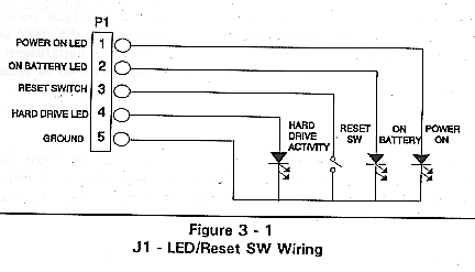
LEDs/Reset Switch
Internal header J1 provides an interface for three LEDs and an external reset switch. The LEDs are:
Power LED is illuminated when power is ON
On Battery LED is illuminated when running on battery power (refer to Power Supply Status description)
Hard Disk LED is illuminated during hard disk activity
The external reset switch provides a method of performing a hard reset of the BC 4000. Figure 3-1 describes the wiring information for this interface.
Power Supply Status
The BC 4000 has a power supply status connector (J4) to monitor the condition of the power supply. This connector would connect to a power supply which can provide the data required by the pin out shown below.
1 - Power Off (output)
2 - Low Battery (input)
3 - A.C. Fail (input) - can cause IRQ 10 or 15 as
configured by JP1 positions 1 - 3.
4 - Power Good (input)
The output on pin 1 is to turn the power supply off. This would typically be done when the A.C. has failed and the backup batteries have reached their discharge state. Pin 2 is an input to the BC 4000 and is low when the batteries have discharged. Pin 3 is an input to the BC 4000 and is low when the A.C. to the power supply has failed and the power supply is running off of the batteries. This condition will cause the On Battery LED to illuminate. Pin 4 is an input to the BC 4000 and is raised high by the Power Supply when its D.C. output voltages are stable and within their limits. All of the signals on J4 are TTL compatible.
Memory
All BC 4000 system memory is provided in 72-pin by 36-bit standard 70ns SIMM modules in 4MB or 16MB versions. Memory size configurations range from 4 MB to 64 MB.
ISA Bus Connector
The ISA Bus connectors on the board use the same pinout and signals as all standard PC/AT bus connectors.
The 16 system hardware interrupts on the BC 4000 are represented in the following table. Interrupts are managed by two standard 8259A Programmable Interrupt Controllers (PICs). Interrupts at IRQ 0 through 7 are located on the main PIC; IRQ 8 through 15 are on the slave PIC.
       Table 3 - 1
  Hardware IRQ Information

IRQ Description                     IRQ Description

0 Timer Click                       1 Keyboard
2 Second PIC Controller             3 COM2
4 COM1                              5 Available
6 Floppy Disk Controller            7 LPT1
8 Real-Time Clock                   9 Redirected IRQ2
10 Available or AC Fail (JP1)      11 Available
12 Available or Mouse (JP5)        13 Math Coprocessor
14 Fixed Disk Controller           15 Available or AC Fail
(JP1)
             Table 2 - 4
     JP1, JP4, JP5 Summary

 FUNCTION                            JP4         JP1
 JP5
                                    /   /       /   /      |
                                  1-2   3-4   1-2   2-3    |


Disable COM1, COM2, and LPT1     ON     ---   ---   ---
---

Disable IDE hardware             ---    ON    ---   ---
---

*COM/LPT/IDE enabled             OFF    OFF   ---   ---
---

A.C. Fail Interrupt on IRQ 10    ---    ---   OFF   ON
---

A.C. Fail Interrupt on IRQ 15    ---    ---   ON    OFF
---

*No A.C. Fail Interrupt          ---    ---   OFF   OFF
---

Mouse on IRQ 12 enabled          ---    ---   ---   ---   ON

*Mouse on IRQ 12 disabled        ---    ---   ---   ---
OFF


* Factory default
               Table 3 - 3
   Switch Settings for Monitors (S1)

Video Mode            SW1   SW2   SW3   SW4   SW5   SW6
SW7   SW8

CGA (with NMI)        ON    ON    ON    ON    OFF   OFF
OFF   *
MDA (with NMI)        OFF   ON    ON    ON    OFF   OFF
OFF   *
MDA (without NMI)     ON    OFF   ON    ON    OFF   OFF
OFF   *
EGA (with NMI)        OFF   OFF   ON    ON    OFF   OFF
OFF   *
EGA (without NMI)     ON    ON    OFF   ON    OFF   OFF
OFF   *
VGA (Color)**         OFF   ON    OFF   ON    OFF   OFF
OFF   *
VGA (Mono)            ON    OFF   OFF   ON    OFF   OFF
OFF   *
8514                  OFF   OFF   OFF   ON    OFF   OFF
OFF   *
NEC 2A                ON    ON    ON    OFF   OFF   OFF
OFF   *
NEC / NEC+            OFF   ON    ON    OFF   OFF   OFF
OFF   *
NEC XL                ON    OFF   ON    OFF   OFF   OFF
OFF   *
NEC 3D                OFF   OFF   ON    OFF   OFF   OFF
OFF   *
NEC 4D /5D            ON    ON    OFF   OFF   OFF   OFF
OFF   *
Portrait              OFF   ON    OFF   OFF   OFF   OFF
OFF   *
Reserved              ON    OFF   OFF   OFF   OFF   OFF
OFF   *
Reserved              OFF   OFF   OFF   OFF   OFF   OFF
OFF   *

* SW8 is OFF for non-interlaced monitors, and ON for
interlaced
monitors.

** Factory default is non-interlaced VGA (color).
                Table 3 - 4
       Reset on Loss of DCD or DSR
            (Switch JP3)


Reset Condition              Shunt Position

                                   1-2   3-4    5-6   7-8

Reset when DSR drops on COM1       ON    OFF    OFF   OFF

Reset when DSR drops on COM2       OFF    ON    OFF   OFF

Reset when DCD drops on COM1       OFF   OFF    ON    OFF

Reset when DCD drops on COM2       OFF   OFF    OFF    ON
                        Table 3 - 5
   Control Panel Connector J1 (5-Pin Header)

Contains connections for remote IDE drive LED, power on LED,
battery
on LED, and external reset switch.

Pin #          Description

1              Resistor pull-up for Power on LED
2              ON Battery LED (running on Battery power)
3              Reset Switch (ground to reset computer)
4              IDE Drive LED
5              Ground
                    Table 3 - 6
      Speaker Connector J2 (4-Pin Header)

For wiring to a panel-mounted speaker and keylock switch

Pin #       Description

1            Speaker data
2            N/C (no connection)
3            Ground
4            +5V (speaker power)
              Table 3 - 7
   Optional Mouse Connector J4 (5-Pin Header)

Pin #     Description

1           DATA
2           N/C (no connection)
3           Ground
4           +5V
5           CLK (Clock)
                          Table 3 - 8
     Floppy Diskette Connector J5 (34-Pin Header)

This 34-pin cable header is pinned-out to use a standard
PC/AT
style floppy disk cable. The drive should be shunted for
single-speed
operation (360 RPM).

Pin #     Description        Pin #       Description

1         GROUND             2          SPEED
3         GROUND             4          N/C
5         GROUND             6          N/C
7         GROUND             8          INDEX
9         GROUND            10          MOTOR ON 1
11        GROUND            12          DRIVE SEL 2
13        GROUND            14          DRIVE SEL 1
15        GROUND            16          MOTOR ON 2
17        GROUND            18          DIRECTION
19        GROUND            20          STOP STEP
21        GROUND            22          WRITE DATA
23        GROUND            24          WRITE GATE
25        GROUND            26          TRACK 0
27        GROUND            28          WRITE PROTECT
29        GROUND            30          READ DATA
31        GROUND            32          SIDE SELECT
33        GROUND            34          DISK CHANGE
                        Table 3 - 9
      IDE Interface Connector J6 (40-Pin Header)


Pin Desc.       Pin Description

 1  RESET        2  GROUND
 3  DATA 7       4  DATA 8
 5  DATA 6       6  DATA 9
 7  DATA 5       8  DATA 10
 9  DATA 4      10  DATA 11
11  DATA 3  	12  DATA 12
13  DATA 2  	14  DATA 13
15  DATA 1  	16  DATA 14
17  DATA 0  	18  DATA 15
19  GROUND  	20  N/C
21  N/C  	22  GROUND
23  IOW   	24  GROUND
25  IOR   	26  GROUND
27  N/C   	28  BALE
29  N/C   	30  GROUND
31  IDINT  	32  N/C
33  SA1   	34  N/C
35  SA0   	36  SA2
37  CS5   	38  HCS1
39  N/C   	40  N/C
                    Table 3 - 10
       Optional Parallel Port, LPT1 J7 (DB25)

A 20-pin ribbon header is provided on the board for
connection
to the optional DB25S parallel port printed circuit board
that
mounts on a rear panel.

Pin #  Description   Pin #  Description

 1  GROUND       2  STROBE
 3  BUSY         4  SELECT
 5  ERROR        6  SLIN
 7  INIT         8  AFT
 9  PAPER OUT   10  ACKNOWLEDGE
11  DATA 0   	12  DATA 1
13  DATA 2   	14  DATA 3
15  DATA 4   	16  DATA 5
17  DATA 6      18  DATA 7
19  GROUND      20  GROUND
                  Table 3 - 11
     COM Port Connector J9 (DB-9), J8 (10-pin header)

The COM1 port is on the rear bracket of the board on a
DSUB-9P
connector. To enable the optional COM2 port, it must be
cabled
to a Cubix interface board. DO NOT cable connector J9 (COM2)
directly
to a DB-9 or DB-25 connector.

Pin #  Description

1  DCD (Data Carrier Detect)
2  RD (Receive Data)
3  TD (Transmit Data)
4  DTR (Data Terminal Ready)
5  GND (Ground)
6  DSR (Data Set Ready)
7  RTS (Request to Send)
8  CTS (Clear to Send)
9  RI (Ring Indicator)
            Table 3 - 12
  Video/Keyboard Mux Connector - J3 (14-Pin Header)

This connector contains the video and keyboard signals. In
some
Cubix systems it can be cabled to an internal video/keyboard
multiplexor
board.


 1  RED          2  GROUND
 3  GREEN        4  GROUND
 5  BLUE         6  GROUND
 7  HSYNC        8  GROUND
 9  VSYNC       10  GROUND
11  KCLK   	12  GROUND
13  KDATA   	14  +5 (FUSED)
                 Table 3 - 13
Keyboard Connector J10 (PS/2 compatible 6-pin Mini-DIN)

Pin #  Description

1  DATA
2  N/C (no connection)
3  Ground
4  +5V
5  CLK (Clock)
6  N/C (no connection)
              Table 3 - 14
        Video Connector J11
   (Standard VGA 15-Pin High-Density Female DSUB)

Pin #  Description

 1   Red
 2   Green
 3   Blue
 4   N/C (no connection)
 5   Ground
 6   Ground
 7   Ground
 8   Ground
 9   N/C (no connection)
10   Ground
11   N/C (no connection)
12   N/C (no connection)
13   VSYNC
14   HSYNC
15   N/C (no connection)
This document, and all Web contents, Copyright © 1997
by Cubix Corp., Carson City, NV, USA.