 |
|
|
|
BC 3030
Chapter 2 - Hardware
Standard Features
System Components
System Interrupts
Video Switch
Reset on Loss of DCD or DSR
Optional LPT1 Port
Optional COM2 and Mouse
Connectors and Signals
Specifications
* 80386SX, 25 MHz processor, and 80387SX Coprocessor socket
* Four standard SIMM sockets to expand memory up to 16MB total DRAM with parity
* Internal header connectors for
- Reset switch
- Hard Drive activity LED
- Power ON LED
- ON Battery Power LED
- Video/Keyboard MUX
- Speaker
- CMOS Battery
- Remotemounted PS/2 mouse connector
- Floppy controller for 5-1/4" and 3-1/2" drives
- IDE hard drive controller, supports two drives
- COM2 serial header
- LPT1 parallel header
* PS/2 compatible keyboard connector
* 8.33/10MHz AT ISA bus timing
* Real time clock
* VGA Video controller
* 8-bit EPROM BIOS
* VLSI Technology, Inc. TOPCAT AT chip set with LIM 4.0 support, supports system and video BIOS in shadow RAM
* Rear Panel Connectors for
- VGA monitor
- COM1
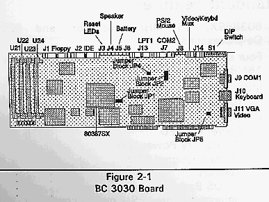
- PS/2 keyboard Figure 2-1
EPROM BIOS
An American Megatrends, Inc. (AMI) system BIOS with embedded setup and hard disk setup utilities resides on the board (27C512 EPROM). At boot time, the data can be transferred to 16bit shadow RAM. This option provides increased system performance, since RAM access is more efficient than EPROM access. (Chapter 3 contains the AMI BIOS documentation.)
Video Controller
The BC 3030 contains an extended high resolution VGA graphics controller (Oak Technology OTI067). With 512K of video memory, this controller supports all standard VGA modes and the following extended modes: 640 x 480 with 256 colors; 800 x 600 with 256 colors; and 1024 x 768 with 16 colors. The connector on the board (J11) is an industry standard VGA connector (15pin highdensity DSubminiature).
Keyboard Controller
The BC 3030 has a PS/2 compatible keyboard controller (8042 or 8742) with the AMI keyboard BIOS. The keyboard controller uses IRQ 1 for its interrupts, and requires no DMA channel.
The keyboard connector on the board (J10) is an industry standard PS/2 compatible 6-pin Mini-DIN connector. The keyboard controller also supports a PS/2 compatible mouse port. The mouse cable and connector are available as an optional item. If added to the board, the mouse port uses IRQ 12.
Video/Keyboard Multiplexer
The BC 3030 has a header connector (J14) for a Cubix internal video/keyboard multiplexor (MUX). Typically, the MUX is used in installations where multiple BC 3030 boards have been integrated into a system with a single monitor and keyboard. Refer to the Video MUX Installation Guide for more information.
IDE Hard Drive Interface
An IDE hard drive interface is included on the BC 3030 for applications that require a hard disk drive. IDE drives include an AT compatible disk controller. The IDE interface circuit will support one or two IDE drives, connected via the internal 40pin ribbon cable header (J2). When adding an IDE drive to the board, use the setup program to select the drive type. See the BC 3030 Setup Program Chapter for information on selecting IDE drive types.
Disabling the IDE Controller
The IDE disk controller can be disabled if necessary in the CMOS setup program. This would be necessary if, for example, a SCSI adapter was installed and the SCSI adapter's hard disk was to be used as a boot device. To completely disable the IDE hardware, a jumper must be placed on jumper block JP4, pins 3-4.
Floppy Disk Controller
The BC 3030 contains a Western Digital 37C65B floppy disk controller. It supports all PC/AT floppy disk configurations. The board has an internal 34pin ribbon cable header (J1) for cabling to the floppy disk drive. The controller is configured for industry standard singlespeed floppy disk drives, and supports up to two of any combination of 5-1/4 or 3-1/2 inch drives. The BIOS setup program must be configured for the proper drives. The floppy controller uses IRQ6 for its interrupt and DRQ2 for its DMA channel.
* The floppy controller on the BC 3030 board cannot be disabled.
Serial and Parallel Ports
Two serial ports and a parallel port are available on the BC 3030. One serial port is accessible through a standard DB-9 connector on the rear bracket (J9). The other serial port (COM2) and the parallel port (LPT1) are accessible internally through header connectors (J7 and J13). All ports comply fully with PC/AT® interrupt and I/O port standards.
The serial and parallel ports may be disabled by placing a jumper on jumper block JP4, pins 1-2. This recovers interrupts at IRQ 3, 4, and 7.
External access to the internal I/O connectors (COM2, LPT1, PS/2 mouse) is accomplished through Cubix supplied interface boards. Refer to the sections Optional LPT1 Port and Optional COM2 and Mouse later in this chapter for more information. Contact the Cubix Sales department to order the serial or parallel port expansion product required to access the mouse, COM2, or LPT1 ports.
Speaker
The BC 3030 has a header connection (J4) for an eight ohm permanent magnet type speaker. The speaker output comes from the output of TIMER 2 through a gate controlled by bit 0 of Port B, which is the standard AT speaker oscillator.
CMOS Battery
The CMOS Battery interface (J5) accepts a 6-volt external battery source to back up the CMOS setup RAM and time of day clock. It is highly recommended that this battery be installed, for without it the BC 3030 requires manual intervention to boot.
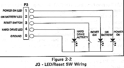
LEDs/Reset Switch
Internal header J3 provides an interface for three LEDs and an external reset switch. The LEDs are:
Power LED is illuminated when power is on
On Battery LED is illuminated when running on battery power (refer to Power Supply Status description)
Hard Disk LED is illuminated during hard disk activity
The external reset switch provides a method of performing a hard reset of the BC 3030. Figure 2-21Figure 2-2 describes the wiring information for this interface.
Power Supply Status
The BC 3030 has a power supply status connector (J6) to monitor the condition of the power supply. This connector would connect to a power supply which can provide the data required by the pin out shown below.
1 - Power Off (output)
2 - Low Battery (input)
3 - A.C. Fail (input)
4 - Power Good (input)
The output on pin 1 is to turn the power supply off. This would typically be done when the A.C. has failed and the backup batteries have reached their discharge state. Pin 2 is an input to the BC 3030 and is low when the batteries have discharged. Pin 3 is an input to the BC 3030 and is low when the A.C. to the power supply has failed and the power supply is running off of the batteries. This condition will cause the On Battery LED to illuminate. Pin 4 is an input to the BC 3030 and is raised high by the Power Supply when its D.C. output voltages are stable and within their limits. All of the signals on J6 are TTL compatible.
TOPCAT Chip Set
A VLSI Technology, Inc. TOPCAT AT chip set implements the memory controller and ISA bus controller functions. This twochip controller set also includes the logic necessary to implement the LIM (Lotus/Intel/Microsoft) Revision 4.0 memory management functions. The chip set includes a battery backed realtime clock and CMOS setup memory. It also contains the interrupt, timer, and DMA controllers and a pagemode DRAM memory controller.
Memory
All BC 3030 system memory is provided in 30-pin by 9-bit standard 70ns SIMM modules. These modules should be installed in the sockets provided. These sockets are labeled as U21, U22, U23, and U24 on Figure 2-1.
Memory size options include 2MB, 4MB, 8MB, 10MB, and 16MB. The configurations supported are represented in Table 2-1.
                   Table 2 - 1
             SIMM Configurations

 U21  U22  U23   U24  TOTAL MEMORY
 1MB  1MB  None  None    2MB
 1MB  1MB  1MB   1MB     4MB
 4MB  4MB  None  None    8MB
 1MB  1MB  4MB   4MB    10MB
 4MB  4MB  4MB   4MB    16MB


Note that the SIMMs must be installed in matching pairs.
Each
pair must reside in either the first two sockets (U21 and
U22)
or the second two sockets (U23 and U24).
ISA Bus Connector
The ISA Bus connectors on the board use the same pinout and signals as all standard PC/AT bus connectors.
The 16 system hardware interrupts on the BC 3030 are represented in the following table. Interrupts are managed by two standard 8259A Programmable Interrupt Controllers (PICs). Interrupts at IRQ 0 through 7 are located on the main PIC; IRQ 8 through 15 are on the slave PIC.
             Table 2-2
  Hardware IRQ Information

IRQ Description                 IRQ Description

0 Timer Click                   1 Keyboard
2 Second PIC Controller         3 COM2
4 COM1                          5 Available
6 Floppy Disk Controller        7 LPT1
8 Real-Time Clock               9 Redirected IRQ2
10 Available or AC Fail (JP1)   11 Available
12 Available or Mouse (JP5)     13 Math Coprocessor
14 Fixed Disk Controller        15 Available or AC Fail
(JP1)
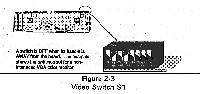
Set the Video Switch to match the monitor. Figure 2-3 shows Video Switch (S1). Table 2-3 shows switch settings for each monitor.
 Table 2-3

 Switch Settings for Monitors

Video           SW1   SW2   SW3   SW4   SW5   SW6   SW7
SW8
Mode

Reserved        OFF   OFF   OFF   OFF   OFF   OFF   OFF    *
Reserved        ON    OFF   OFF   OFF   OFF   OFF   OFF    *
Portrait        OFF   ON    OFF   OFF   OFF   OFF   OFF    *
NEC 4D/5D       ON    ON    OFF   OFF   OFF   OFF   OFF    *
NEC 3D          OFF   OFF   ON    OFF   OFF   OFF   OFF    *
NEC XL          ON    OFF   ON    OFF   OFF   OFF   OFF    *
NEC/NEC+        OFF   ON    ON    OFF   OFF   OFF   OFF    *
NEC 2A          ON    ON    ON    OFF   OFF   OFF   OFF    *
8514            OFF   OFF   OFF   ON    OFF   OFF   OFF    *
VGA (mono)      ON    OFF   OFF   ON    OFF   OFF   OFF    *
VGA             OFF   ON    OFF   ON    OFF   OFF   OFF    *

*  SW8 is OFF for non-interlaced monitors, and ON for
interlaced
monitors.

Factory default is non-interlaced VGA (color).
* The BC 3030 video outputs are analog and will only function with analog compatible monitors.
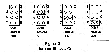
The BC 3030 board can be configured to perform a hardware reset when the Data Carrier Detect (DCD) or Data Set Ready (DSR) signal changes from true to false. Jumpers on jumper block JP2 determine which signal from which COM port will reset the board. The figure below shows jumper block JP2 with a jumper in each position. Figure 2-4.
* A jumper across pins 1 and 2 resets the hardware when the DCD signal drops on COM1.
* A jumper across pins 3 and 4 resets the hardware when the DSR signal drops on COM1.
* A jumper across pins 5 and 6 resets the hardware when the DCD signal drops on COM2.
* A jumper across pins 7 and 8 resets the hardware when the DSR signal drops on COM2.
To disable reset on loss of DCD or DSR, remove all of the jumpers. This can also be accomplished by placing a jumper across pins 2 and 4 and a jumper across pins 6 and 8 (factory default).
Only one jumper for each COM port should be installed on the jumper block. Do not put jumpers simultaneously on pins 1, 2, 3, and 4. Do not put jumpers simultaneously on pins 5, 6, 7, and 8.
                       Table 2-4
                    Jumper Summary


JP1    AC Fail  Interrupt Select
       1-2               IRQ 10
       2-3               IRQ 15
       NONE           None selected (factory default)

JP2    COM Port Reset Select
       1-2               Reset on COM1 DCD
       3-4               Reset on COM1 DSR
       5-6               Reset on COM2 DCD
       7-8               Reset on COM2 DSR
       2-4 & 6-8     No reset selected (factory default)
       NONE              No reset selected

JP3    Not Used

JP4    COM/IDE Disable
       1-2               Disable COM1, COM2, and LPT1 Ports
       3-4               Disable IDE hardware
       NONE              Hardware is enabled (factory
       default)

       *  To recover IRQ 14, all IDE drives must be removed
       from the
       40-pin header  cable.

JP5    Mouse Interrupt Select
       1-2             IRQ 12 is used for the PS/2 Mouse
       Port
       NONE            IRQ 12 is available for use by other
       cards
                       (factory default)
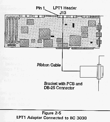
A parallel port may optionally be added to function as LPT1 of the BC 3030. This requires a Cubix LPT1 printed circuit board (PCB) adapter and bracket, a panel opening where the DB-25 connector can be installed, and a 20-conductor ribbon cable.
INSTALLATION
Warning: Turn off the power to the system before beginning this procedure.
1. Install the Cubix LPT1 adapter in a panel opening on the system. Typically, an opening provided for an empty board space is dedicated to the LPT1 connector. In this case, install the bracket next to the BC 3030 board requiring the LPT1 port and tighten the screw firmly.
Alternately, if the LPT1 connector is being installed into a Cubix auxiliary junction panel, the bracket provided with the LPT1 adapter should be removed. Unscrew the connector from the bracket and install the adapter into the desired panel opening.
2. Connect one end of the 20conductor ribbon cable to the LPT1 header (J13) on the BC 3030 board. The pin-one side of the ribbon cable is marked with a colored (blue or red) stripe. Pin one on the BC 3030 header is labeled with a triangular arrowhead (Ú). Align the pin-one side of the ribbon cable with pin one on the header.
3. Connect the other end of the ribbon cable to the LPT1 adapter. Pin one on the adapter is labeled with a triangular arrowhead. Align the pin-one side of the ribbon cable with pin one on the adapter.
4. Plug the peripheral device's cable into the DB25 connector. Figure 2-5.
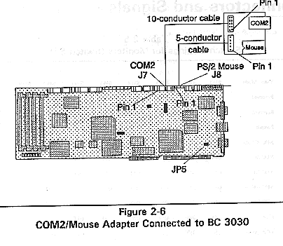
A second serial port may optionally be added to function as COM2 of the BC 3030. A PS/2 mouse input port may also be added. This requires a Cubix printed circuit board (PCB) adapter and bracket, and a single panel opening where the DB-9 and Mini-DIN 6 can be installed. Both the COM2 and the mouse interfaces are provided on the same PCB adapter. To connect COM2 requires a 10-conductor ribbon cable; the mouse port requires a 5-conductor cable.
INSTALLATION
Warning: Turn off the power to the system before beginning this procedure.
1. Install the Cubix PCB adapter in a panel opening on the system. Typically, an opening provided for an empty board space is dedicated to the COM2 and mouse connectors. In this case, install the bracket next to the BC 3030 board requiring the COM2/mouse port, and tighten the screw firmly.
Alternately, if the COM2 and mouse connectors are being installed into a Cubix auxiliary junction panel, the bracket provided with the COM2/mouse adapter should be removed. Unscrew the connectors from the bracket and install the adapter into the desired opening.
2. Connect one end of the 10conductor ribbon cable to the COM2 header (J7) on the BC 3030 board. The pin-one side of the ribbon cable is marked with a colored (blue or red) stripe. Pin one on the BC 3030 header is labeled with a triangular arrowhead (Ú). Align the pin-one side of the ribbon cable with pin one on the header.
3. Connect the opposite end of the 10-conductor cable to the 10-pin header on the Cubix adapter board. Pin one on the adapter is indicated in Figure 2-6. Align the pin-one side of the ribbon cable with pin one of the 10-pin header on the adapter board.
4. Connect one end of the 5-conductor cable to the PS/2 mouse header (J8) on the BC 3030 board. Pin numbers one through five are indicated on the cable connector. Pin one of the BC 3030 header is indicated in Figure 2-6. Align pin one of the cable connector with pin one on the header.
5. Connect the opposite end of the 5-conductor cable to the 5-pin header on the Cubix adapter board. On the adapter board, pin one of the 5-pin header is the closest pin to the edge of the board. Align pin one of the cable connector with pin one on the header.
6. If COM2 is to be used, plug the peripheral device's cable into the DB9 connector.
7. If a mouse if to be used, plug the mouse connector into the Mini-DIN 6.
! Use jumper block JP5 to enable the mouse interrupt (IRQ 12). Also check advanced CMOS setup to make sure mouse support is enabled in the BIOS.
         Table 2-5
 Switch Settings for Monitors

Video           SW1   SW2   SW3   SW4   SW5   SW6   SW7
SW8
Mode

Reserved        OFF   OFF   OFF   OFF   OFF   OFF   OFF    *
Reserved        ON    OFF   OFF   OFF   OFF   OFF   OFF    *
Portrait        OFF   ON    OFF   OFF   OFF   OFF   OFF    *
NEC 4D/5D       ON    ON    OFF   OFF   OFF   OFF   OFF    *
NEC 3D          OFF   OFF   ON    OFF   OFF   OFF   OFF    *
NEC XL          ON    OFF   ON    OFF   OFF   OFF   OFF    *
NEC/NEC+        OFF   ON    ON    OFF   OFF   OFF   OFF    *
NEC 2A          ON    ON    ON    OFF   OFF   OFF   OFF    *
8514            OFF   OFF   OFF   ON    OFF   OFF   OFF    *
VGA (mono)      ON    OFF   OFF   ON    OFF   OFF   OFF    *
VGA             OFF   ON    OFF   ON    OFF   OFF   OFF    *

*  SW8 is OFF for non-interlaced monitors, and ON for
interlaced
monitors.

Factory default is non-interlaced VGA (color).
                  Table 2-6
     Floppy Diskette Connector J1 (34-Pin Header)

This 34-pin cable header is pinned-out to use a standard
PC/AT
style floppy disk cable.  The drive should be shunted for
single-speed
operation (360 RPM).

Pin #  Description  Pin #  Description

1  GROUND  	2  SPEED
3  GROUND  	4  N/C
5  GROUND  	6  N/C
7  GROUND  	8  INDEX
9  GROUND  	10  MOTOR ON 1
11  GROUND  	12  DRIVE SEL 2
13  GROUND  	14  DRIVE SEL 1
15  GROUND  	16  MOTOR ON 2
17  GROUND  	18  DIRECTION
19  GROUND  	20  STOP STEP
21  GROUND  	22  WRITE DATA
23  GROUND  	24  WRITE GATE
25  GROUND  	26  TRACK 0
27  GROUND  	28  WRITE PROTECT
29  GROUND  	30  READ DATA
31  GROUND  	32  SIDE SELECT
33  GROUND  	34  DISK CHANGE
        Table 2-7
 IDE Interface Connector J2 (40-Pin Header)

Pin Desc.       Pin Description

1  RESET   	2  GROUND
3  DATA 7  	4  DATA 8
5  DATA 6  	6  DATA 9
7  DATA 5  	8  DATA 10
9  DATA 4  	10  DATA 11
11  DATA 3  	12  DATA 12
13  DATA 2  	14  DATA 13
15  DATA 1  	16  DATA 14
17  DATA 0  	18  DATA 15
19  GROUND  	20  N/C
21  N/C  	22  GROUND
23  IOW   	24  GROUND
25  IOR   	26  GROUND
27  N/C   	28  BALE
29  N/C   	30  GROUND
31  IDINT  	32  N/C
33  SA1   	34  N/C
35  SA0   	36  SA2
37  CS5   	38  HCS1
39  N/C   	40  N/C
            Table 2-8
   Control Panel Connector J3 (5-Pin Header)

Contains connections for remote IDE drive LED, power on LED,
battery
on LED, and external reset switch.

Pin #  Description

1  Resistor pull-up for Power on LED
2  ON Battery LED (running on Battery power)
3  Reset Switch (ground to reset computer)
4  IDE Drive LED
5  Ground
          Table 2-9
    Speaker Connector J4 (4-Pin Header)

For wiring to a panel-mounted speaker and keylock switch

Pin #  Description

1  Speaker data
2  N/C (no connection)
3  Ground
4  +5V (speaker power)
                   Table 2-10
 CMOS Battery Connector J5 (2-Pin Polarized Header)

Connects to a battery holder with four alkaline AA cells,
yielding
a 6-Volt battery pack.

Pin #  Description

1  Positive
2  Negative
                Table 2-11
      Optional Mouse Connector J8 (5-Pin Header)

Pin #  Description

1  DATA
2  N/C (no connection)
3  Ground
4  +5V
5  CLK (Clock)
                 Table 2-12
 COM Port Connector J9 (DB-9), J7 (10 pin header)

The COM1 port is on the rear bracket of the board on a
DSUB-9P
connector.  To enable the optional COM2 port, it must be
cabled
to a Cubix interface board.  DO NOT cable connector J7
(COM2)
directly to a DB-9 or DB-25 connector.

Pin #  Description

1  DCD (Data Carrier Detect)
2  RD (Receive Data)
3  TD (Transmit Data)
4  DTR (Data Terminal Ready)
5  GND (Ground)
6  DSR (Data Set Ready)
7  RTS (Request to Send)
8  CTS (Clear to Send)
9  RI (Ring Indicator)
               Table 2-13
   Keyboard Connector J10 (PS/2 compatible 6-pin Mini-DIN)

Pin #  Description

1  DATA
2  N/C (no connection)
3  Ground
4  +5V
5  CLK (Clock)
6  N/C (no connection)
      Table 2-14
  Video Connector J11

(Standard VGA 15-Pin High-Density Female DSUB)

Pin #  Description

1   Red
2   Green
3   Blue
4   N/C (no connection)
5   Ground
6   Ground
7   Ground
8   Ground
9   N/C (no connection)
10   Ground
11   N/C (no connection)
12   N/C (no connection)
13   VSYNC
14   HSYNC
15   N/C (no connection)
         Table 2-15
   Optional Parallel Port, LPT1 J13 (DB25)

A 20-pin ribbon header is provided on the board for
connection
to the optional DB25S parallel port printed circuit board
that
mounts on a rear panel.

Pin #  Description   Pin #  Description

1  GROUND   	2  STROBE
3  BUSY     	4  SELECT
5  ERROR   	6  SLIN
7  INIT     	8  AFT
9  PAPER OUT  	10  ACKNOWLEDGE
11  DATA 0   	12  DATA 1
13  DATA 2   	14  DATA 3
15  DATA 4   	16  DATA 5
17  DATA 6      18  DATA 7
19  GROUND      20  GROUND
          Table 2-16
  Video/Keyboard Mux Connector - J14 (14-Pin Header)

This connector contains the video and keyboard signals.  In
some
Cubix systems it can be cabled to an internal video/keyboard
multiplexer
board.

1  RED    	2  GROUND
3  GREEN   	4  GROUND
5  BLUE   	6  GROUND
7  HSYNC   	8  GROUND
9  VSYNC   	10  GROUND
11  KCLK   	12  GROUND
13  KDATA   	14  +5 (FUSED)
Microprocessors
80386SX, 25MHz
80387SX, 25MHz (Optional)
Real Time CMOS Clock
Clock rate: 32.768 KHz
Power Requirements
Power: 12.7 - 13.7 watts
+5 VDC @ 2.2 amps maximum (without 80387SX)
+5 VDC @ 2.5 amps maximum (with 80387SX)
+12 VDC @ 0.03 amps maximum
-12 VDC @ 0.03 amps maximum
Operating Environment
0 - 500C
0 - 80% noncondensing
Floppy Controller
Supports one or two 3.5" or 5.25" drives
"AT" Chip Set
VLSI Technology, Inc. "TOPCAT" CHIPSET
Single and 2-way page mode interleave
LIM EMS 4.0 memory controller
Hard Disk Controller
Supports one or two IDE hard drives
COM1 Port
16C552 Controller with 8250 compatibility
Transmission Rate: 50-115 KBITS/sec, asynchronous
Data Bits: 8, 7, 6, or 5
Parity: None, Odd, Even
Stop Bits: 1, 1-1/2, 2
Access: DB-9 on board mounting bracket
COM2 Port
16C552 Controller with 8250 compatibility
Transmission Rate: 50-115 KBITS/sec, asynchronous
Data Bits: 8, 7, 6, or 5
Parity: None, Odd, Even
Stop Bits: 1, 1-1/2, 2
Access: 10-pin ribbon header, requires optional PCB to convert to DB-9.
LPT1 Port
Centronics compatible
Access: 20-pin ribbon header, requires optional PCB to convert to DB-25.
Video Port
Super VGA video controller with .5MB of video memory
Max Resolution: 1024 x 768, 16 colors
Access: High Density DB-15 on board mounting bracket
Keyboard Port
PS/2 compatible keyboard controller
Access: Mini-DIN 6 on board mounting bracket
Mouse Port
PS/2 compatible mouse port
Access: 5-pin header, requires optional PCB to convert to Mini-DIN 6 connector.
Memory Configuration
Supports two or four 30-pin memory SIMMs
Standard memory is 2MB
Expandable to 4MB, 8MB, 10MB, or 16MB
Internal Header Connections for:
Reset switch
Hard drive activity LED
Power on LED
On battery power LED
Power supply status interface
Video/keyboard MUX
Speaker
CMOS battery
COM2
LPT1
PS/2 Mouse
Floppy drive
IDE hard drive
This document, and all Web contents, Copyright © 1997
by Cubix Corp., Carson City, NV, USA.