 |
|
|
|
QL 3001
Quick Reference Guide
This header requires a optional I/O adapter from Cubix. Attempting to connect a device directly to this connector will damage the board.
| 1 | DCD (data carrier detect) |
| 2 | RD (receive data) |
| 3 | TD (transmit data) |
| 4 | DTR (data terminal ready) |
| 5 | GND (ground) |
| 6 | DSR (data set ready) |
| 7 | RTS (request to send) |
| 8 | CTS (clear to send) |
| 9 | RI (ring indicator) |
The VGA versions of the QL 3000 Series boards use auto-sensing to detect the video type. Leave switch 2 of switch block SW1 ON. Previous revisions of the QL 3001 board used either MDA or CGA video mode. Switch 2 of switch block SW1 selects the video mode.
| Mode | SW1 | SW2 |
| CGA | n/a | ON |
| Mono | n/a | OFF |
| VGA | n/a | ON |
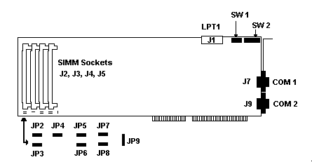
Each QL 3001 board houses a four position DIP switch (SW1). Switches 3 and 4 of SW1 select the base I/O address used by the server driver to communicate with the QL 3001 processors. The QL interface requires eight consecutive I/O ports beginning with the base I/O address.
The I/O addresses selected must not be assigned to any non-QL 3000 Series devices installed in the file server or bridge hosting the QL 3000 boards. However, all of the QL 3000 Series boards installed in this host should have the same base l/O address.
| Address | SW3 | SW4 |
| 220 | ON | ON |
| 230 | ON | OFF |
| 320 | OFF | ON |
| 330 | OFF | OFF |
Each node on a Novell network must be identified by a unique address. This address consists of two parts: a network number and a node number. When the Cubix server driver is installed, it must be assigned a unique network number. Each QL 3000 series node to be supported by the server driver must be assigned a unique node number. The node number is selected by a DIP switch (SW2) on the QL 3000 board. Valid node numbers range from 1 to 250. It is recommended that the QL 3001 node numbers be assigned consecutively beginning with node number 1 as this will maximize network performance.
The QL 3001 board uses an eight position DIP switch to select the node number for each board. A switch is OFF when its handle is away from the board.
| 001 | 8 off | 030 | 3,4 off | 05F | 2,4,5,6,7,8 |
| 002 | 7 | 031 | 3,4,8 | 060 | 2,3 |
| 003 | 7,8 | 032 | 3,4,7 | 061 | 2,3,8 |
| 004 | 6 | 033 | 3,4,7,8 | 062 | 2,3,7 |
| 005 | 6,8 | 034 | 3,4,6 | 063 | 2,3,7,8 |
| 006 | 6,7 | 035 | 3,4,6,8 | 064 | 2,3,6 |
| 007 | 6,7,8 | 036 | 3,4,6,7 | 065 | 2,3,6,8 |
| 008 | 5 | 037 | 3,4,6,7,8 | 066 | 2,3,6,7 |
| 009 | 5,8 | 038 | 3,4,5 | 067 | 2,3,6,7,8 |
| 00A | 5,7 | 039 | 3,4,5,8 | 068 | 2,3,5 |
| 00B | 5,7,8 | 03A | 3,4,5,7 | 069 | 2,3,5,8 |
| 00C | 5,6 | 03B | 3,4,5,7,8 | 06A | 2,3,5,7 |
| 00D | 5,6,8 | 03C | 3,4,5,6 | 06B | 2,3,5,7,8 |
| 00E | 5,6,7 | 03D | 3,4,5,6,8 | 06C | 2,3,5,6 |
| 00F | 5,6,7,8 | 03E | 3,4,5,6,7 | 06D | 2,3,5,6,8 |
| 010 | 4 | 03F | 3,4,5,6,7,8 | 06E | 2,3,5,6,7 |
| 011 | 4,8 | 040 | 2 | 06F | 2,3,5,6,7,8 |
| 012 | 4,7 | 041 | 2,8 | 070 | 2,3,4 |
| 013 | 4,7,8 | 042 | 2,7 | 071 | 2,3,4,8 |
| 014 | 4,6 | 043 | 2,7,8 | 072 | 2,3,4,7 |
| 015 | 4,6,8 | 044 | 2,6 | 073 | 2,3,4,7,8 |
| 016 | 4,6,7 | 045 | 2,6,8 | 074 | 2,3,4,6 |
| 017 | 4,6,7,8 | 046 | 2,6,7 | 075 | 2,3,4,6,8 |
| 018 | 4,5 | 047 | 2,6,7,8 | 076 | 2,3,4,6,7 |
| 019 | 4,5,8 | 048 | 2,5 | 077 | 2,3,4,6,7,8 |
| 01A | 4,5,7 | 049 | 2,5,8 | 078 | 2,3,4,5 |
| 01B | 4,5,7,8 | 04A | 2,5,7 | 079 | 2,3,4,5,8 |
| 01C | 4,5,6 | 04B | 2,5,7,8 | 07A | 2,3,4,5,7 |
| 01D | 4,5,6,8 | 04C | 2,5,6 | 07B | 2,3,4,5,7,8 |
| 01E | 4,5,6,7 | 04D | 2,5,6,8 | 07C | 2,3,4,5,6 |
| 01F | 4,5,6,7,8 | 04E | 2,5,6,7 | 07D | 2,3,4,5,6,8 |
| 020 | 3 | 04F | 2,5,6,7,8 | 07E | 2,3,4,5,6,7 |
| 021 | 3,8 | 050 | 2,4 | 07F | 2,3,4,5,6,7,8 |
| 022 | 3,7 | 051 | 2,4,8 | 080 | 1 |
| 023 | 3,7,8 | 052 | 2,4,7 | 081 | 1,8 |
| 024 | 3,6 | 053 | 2,4,7,8 | 082 | 1,7 |
| 025 | 3,6,8 | 054 | 2,4,6 | 083 | 1,7,8 |
| 026 | 3,6,7 | 055 | 2,4,6,8 | 084 | 1,6 |
| 027 | 3,6,7,8 | 056 | 2,4,6,7 | 085 | 1,6,8 |
| 028 | 3,5 | 057 | 2,4,6,7,8 | 086 | 1,6,7 |
| 029 | 3,5,8 | 058 | 2,4,5 | 087 | 1,6,7,8 |
| 02A | 3,5,7 | 059 | 2,4,5,8 | 088 | 1,5 |
| 02B | 3,5,7,8 | 05A | 2,4,5,7 | 089 | 1,5,8 |
| 02C | 3,5,6 | 05B | 2,4,5,7,8 | 08A | 1,5,7 |
| 02D | 3,5,6,8 | 05C | 2,4,5,6 | 08B | 1,5,7,8 |
| 02E | 3,5,6,7 | 05D | 2,4,5,6,8 | 08C | 1,5,6 |
| 02F | 3,5,6,7,8 | 05E | 2,4,5,6,7 | 08D | 1,5,6,8 |
The QL 3001 is equipped with a minimum of 2 MB of RAM. The QL 3001 board's RAM resides in 30-pin SIMM's. To add memory, install standard SlMMs or Cubix SlMMs in sockets J2 through J5, and set jumpers JP2 through JP8 to match the memory configuration.
| Total Memory in MB |
SIMM Type in socket |
Pins Jumpered on Jumper Block |
| J2 | J3 | J4 | J5 | JP2 | JP3 | JP4 | JP5 | JP6 | JP7 | JP8 | |
| 2 | CBX | CBX | CBX | CBX | 1-2 | 1-2 | 1-2 | 1-2 | 1-2 | 1-2 | 1-2 |
| 2 | 1X9 | 1X9 | - | - | 2-3 | 2-3 | 2-3 | 2-3 | 2-3 | 2-3 | 2-3 |
| 3 | CBX | CBX | 1X9 | 1X9 | 1-2 | 1-2 | 1-2 | 2-3 | 1-2 | 2-3 | 1-2 |
| 4 | 1X9 | 1X9 | 1X9 | 1X9 | 2-3 | 2-3 | 2-3 | 2-3 | 2-3 | 2-3 | 2-3 |
| 8 | 4X9 | 4X9 | - | - | 2-3 | 2-3 | 2-3 | 2-3 | 2-3 | 2-3 | 2-3 |
| 9 | CBX | CBX | 4x9 | 4x9 | 1-2 | 1-2 | 1-2 | 2-3 | 1-2 | 2-3 | 1-2 |
| 10 | 4x9 | 4x9 | 1x9 | 1x9 | 2-3 | 2-3 | 2-3 | 2-3 | 2-3 | 2-3 | 2-3 |
| 16 | 4x9 | 4x9 | 4x9 | 4x9 | 2-3 | 2-3 | 2-3 | 2-3 | 2-3 | 2-3 | 2-3 |
CBX = A Cubix SIMM, 512K
1x9 = A standard 1x9 SIMM
4x9 = A standard 4x9 SIMM
1-2 = Set jumper accross pins 1 and 2
2-3 = Set jumper accross pins 2 and 3
| 00000 - 9FFFF | System DRAM Memory |
| A0000 - BFFFF | VGA Video Memory |
| C0000 - C7FFF | VGA Video BIOS Copied to Shadow RAM |
| C8000 - CBFFF | Diskless Download Code |
| CC000 - EDFFF | Not used, can be used for EMS |
| EE000 - EFFFF | 8K Dual-Port-RAM |
| F0000 - F7FFF | Not used, can be used for EMS |
| F8000 - FFFFF | Quadtel System BIOS Copied to Shadow RAM |
| 100000 - FFFFFF | Extended DRAM, up to 16 MB |
| 000 - 00F | DMA 1 |
| 020 - 021 | PIC 1 |
| 040 - 043 | Timer |
| 060,064 | 8742 Keyboard Controller |
| 061 | Port B |
| 070 - 071 | CMOS RAM & NMI Mask Register |
| 080 | Manufacturing Hex Display |
| 081 - 08F | DMA Page Registers |
| 0A0 - 0A1 | PIC 2 |
| 0C0 - 0DF | DMA 2 |
| 2F8 - 2FF | COM 2 |
| 300 - 302 | QL 3001 Command/Status |
| 303 | QL 3001 Terminal Emulation Register |
| 378 - 37F | LPT 1 |
| 3B0 - 3DF | VGA |
| 3F8 - 3FF | COM 1 |
| 46E8,102 | VGA Configuration Ports |
| NMI | Parity/VGA |
| 0 | Timer |
| 1 | Keyboard |
| 2 | Cascaded Input for PIC 2 |
| 3 | COM 2 |
| 4 | COM 1 |
| 5 | Broadcast Interrupt from Fileserver |
| 6 | Transmit Interrupt from Fileserver |
| 7 | LPT 1 |
| 8 | Real Time Clock |
| 9 | VGA |
| 10 | Receive Interrupt from Fileserver |
| 11 | Not Used |
| 12 | Not Used |
| 13 | Numeric Co-Processor Interrupt |
| 14 | Not Used |
| 15 | Not Used |
No DMA channels are used by the QL 3001.
This document, and all BBS contents, Copyright © 1997 by Cubix Corp., Carson City, NV, USA.