QL 2200 Series
Quick Reference Guide
QL 2201
Board Connectors, Descriptions, and Pinouts
| 1-1 |
J6 LPT1 (20 pin header) ( Requires optional
Cubix I/O Adapter) |
| 1-2 |
J10 COM2 (DB9) |
| 1-3 |
J11 Junction Box or Async Cable (honda 36) |
Board Jumpers, Descriptions and settings
| 2-1 |
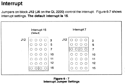
JP12 Interrupt |
| 2-2 |
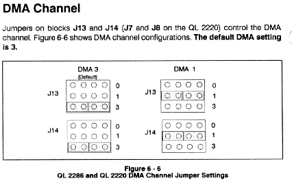
JP13-14 DMA |
Board Switches, Descriptions and settings.
| 3-1 |
SW1 I/O Address, 290 range |
| 3-2 |
I/O Address, 120 range |
Junction Box Connectors and switches
| 1-3 |
J1 To QL Board (honda 36) |
| 1-2 |
COM1 on Junction Box (DB9) |
| 1-5 |
EGA Video on Junction Box (DB9) |
| 1-4 |
Kybd on Junction Box (DIN5) |
| 3-1 |
SW1 Video selection |
Misc.
QL 2286
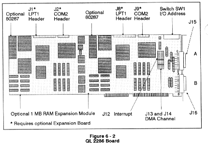
Board Connectors, Descriptions, and Pinouts
| 1-1 |
J1 * Processor A, LPT1 (20 pin header) |
| 1-1 |
J8 * Processor B, LPT1 (20 pin header) |
| 1-7 |
J2 * Processor A, COM2 (10 pin header) |
| 1-7 |
J9 * Processor B, COM2 (10 pin header) |
| 1-3 |
J15 Processor A, to Junction Box |
| 1-3 |
J11 Processor B, to Junction Box |
( * = Requires optional Cubix I/O Adapter)
Board Jumpers, Descriptions and settings
| 2-1 |
JP12 Interrupt |
| 2-2 |
JP13-14 DMA |
Board Switches, Descriptions and settings.
| 3-2 |
SW1 I/O Address, 290 range |
| 3-3 |
I/O Address, 120 range |
Junction Box Connectors and switches
| 1-3 |
J1 To QL Board (36 pin honda connector) |
| 1-2 |
COM1 on Junction Box (DB9) |
| 1-5 |
EGA Video on Junction Box (DB9) |
| 1-4 |
Kybd on Junction Box (DIN5) |
| 3-1 |
SW1 Video selection |
Misc.
QL 2210
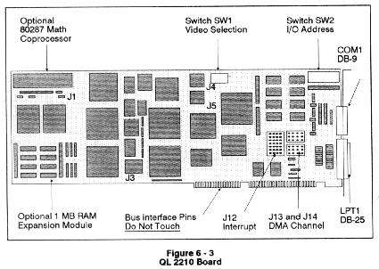
Board Connectors, Descriptions, and Pinouts
| 1-2 |
J1 COM1 (DB9) |
| 1-6 |
J2 LPT1 (DB25) |
Board Jumpers, Descriptions and settings
| 2-1 |
JP12 Interrupt |
| 2-2 |
JP13-14 DMA |
Board Switches, Descriptions and settings.
| 3-2 |
SW1 Video Select |
| 3-3 |
I/O Address, 120 range |
MISC.
QL 2220
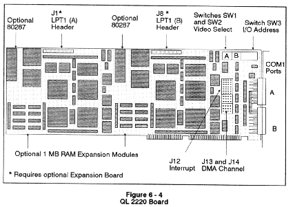
Board Connectors, Descriptions, and Pinouts
| 1-1 |
J1 * Processor A, LPT1 (20 pin header) |
| 1-1 |
J8 * Processor B, LPT1 (20 pin header) |
| 1-2 |
J15 Processor A, COM1 (DB9) |
| 1-2 |
J16 Processor B, COM1 (DB9) |
( * = Requires optional Cubix I/O Adapter)
Board Jumpers, Descriptions and settings
| 2-1 |
JP12 Interrupt |
| 2-2 |
JP13-14 DMA |
Board Switches, Descriptions and settings.
| 3-1 |
SW1 Video Select, processor A |
| 3-1 |
SW2 Video Select, processor B |
| 3-2 |
SW3 I/O Address, 290 range |
| 3-3 |
I/O Address, 120 range |
Misc.
Peripheral Junction Box
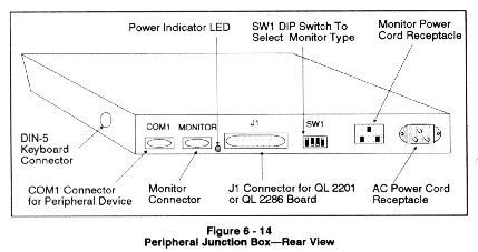
FIGURE 1-1 * LPT1 * 20 pin header (REQUIRES I/O ADAPTER)
This header requires a I/O adapter to make the LPT port functional. The adapter is
available from Cubix. The adapter has a standard PC style DB25 LPT connector (see fig. 1-6
for the adapters connector details). Attempt- to connect a device directly to this
connector will damage the board.
FIGURE 1-2 * COM PORT * (DB9 connector)
| 1 |
DCD (data carrier detect) |
| 2 |
RD (receive data) |
| 3 |
TD (transmit data) |
| 4 |
DTR (data terminal ready) |
| 5 |
GND (ground) |
| 6 |
DSR (data set ready) |
| 7 |
RTS (request to send) |
| 8 |
CTS (clear to send) |
| 9 |
RI (ring indicator) |
FIGURE 1-3 * QL to Junction Box Cable *
(Honda 36 pin connector)
This is a special built cable. It is available from Cubix in standard or custom
lengths. The pinout for this cable is not available.
FIGURE 1-4 * KYBD Connector on Peripherial Junction Box
| 1 |
Kybd clock |
| 2 |
Kybd data |
| 3 |
Kybd reset |
| 4 |
Ground |
| 5 |
+5 Volts |
FIGURE 1-5 * EGA Video on Peripherial Junction Box
| 1 |
Ground |
| 2 |
S. Red |
| 3 |
Red |
| 4 |
Green |
| 5 |
Blue |
| 6 |
S. Green/intensity |
| 7 |
S. Blue/mono video |
| 8 |
Horizontal Drive |
| 9 |
Vertical Drive |
FIGURE 1-6 * LPT1 * (DB25 connector)
| 1 |
strobe |
2 |
data bit 0 |
| 3 |
data bit 1 |
4 |
data bit 2 |
| 5 |
data bit 3 |
6 |
data bit 4 |
| 7 |
data bit 5 |
8 |
data bit 6 |
| 9 |
data bit 7 |
10 |
acknowledge |
| 11 |
+busy |
12 |
+paper end |
| 13 |
+select |
14 |
-auto feed |
| 15 |
-error |
16 |
-init. printer |
| 17 |
-select input |
18-25 |
Ground |
FIGURE 1-7 * COM2 Header * 20 pin header
(REQUIRES I/O ADAPTER)
This header requires a I/O adapter to make the COM2 port functional. The adapter is
available from Cubix. The adapter has a standard PC style DB9 COM connector (see fig. 1-2
for the adapters connector detail). Attempting to connect a device directly to this
connector will damage the board.
FIGURE 2-1 * Interrupt jumpers
FIGURE 2-2 * DMA Jumpers
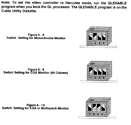
FIGURE 3-1 * Video Select Switch
FIGURE 3-2 * I/O Address Settings, starting at 290.
|
QL 2220
|
QL 2210
|
ADD
|
QL 2286
|
QL 2201
|
| |
|
|
290
|
1,3,6 off
|
1,3,6 off
|
292
|
|
1,3,6,9
|
294
|
1,3,6,8
|
1,3,6,8
|
296
|
|
1,3,6,8,9
|
298
|
1,3,6,7
|
1,3,6,7
|
29A
|
|
1,3,6,7,9
|
29C
|
1,3,6,7,8
|
1,3,6,7,8
|
29E
|
|
1,3,6,7,8,9
|
2A0
|
1,3,5
|
1,3,5
|
2A2
|
|
1,3,5,9
|
2A4
|
1,3,5,8
|
1,3,5,8
|
2A6
|
|
1,3,5,8,9
|
2A8
|
1,3,5,7
|
1,3,5,7
|
2AA
|
|
1,3,5,7,9
|
2AC
|
1,3,5,7,8
|
1,3,5,7,8
|
2AE
|
|
1,3,5,7,8,9
|
2B0
|
1,3,5,6
|
1,3,5,6
|
2B2
|
|
1,3,5,6,9
|
2B4
|
1,3,5,6,8
|
1,3,5,6,8
|
2B6
|
|
1,3,5,6,8,9
|
2B8
|
1,3,5,6,7
|
1,3,5,6,7
|
2BA
|
|
1,3,5,6,7,9
|
2BC
|
1,3,5,6,7,8
|
1,3,5,6,7,8
|
2BE
|
|
1,3,5,6,7,8,9
|
2C0
|
1,3,4
|
1,3,4
|
2C2
|
|
1,3,4,9
|
2C4
|
1,3,4,8
|
1,3,4,8
|
2C6
|
|
1,3,4,8,9
|
2C8
|
1,3,4,7
|
1,3,4,7
|
2CA
|
|
1,3,4,7,9
|
2CC
|
1,3,4,7,8
|
1,3,4,7,8
|
2CE
|
|
1,3,4,7,8,9
|
| |
|
|
* All switch numbers are for the OFF position.
FIGURE 3-3 * I/O Address Settings, starting at 120
|
QL 2220
|
QL 2210
|
ADD
|
QL 2286
|
QL 2201
|
120
|
2,5 off
|
2,5 off
|
122
|
|
2,5,9
|
124
|
2,5,8
|
2,5,8
|
126
|
|
2,5,8,9
|
128
|
2,5,7
|
2,5,7
|
12A
|
|
2,5,7,9
|
12C
|
2,5,7,8
|
2,5,7,8
|
12E
|
|
2,5,7,8,9
|
130
|
2,5,6
|
2,5,6
|
132
|
|
2,5,6,9
|
134
|
2,5,6,8
|
2,5,6,8
|
136
|
|
2,5,6,8,9
|
138
|
2,5,6,7
|
2,5,6,7
|
13A
|
|
2,5,6,7,9
|
13C
|
2,5,6,7,8
|
2,5,6,7,8
|
13E
|
|
2,5,6,7,8,9
|
140
|
2,4
|
2,4
|
142
|
|
2,4,9
|
144
|
2,4,8
|
2,4,8
|
146
|
|
2,4,8,9
|
148
|
2,4,7
|
2,4,7
|
14A
|
|
2,4,7,9
|
14C
|
2,4,7,8
|
2,4,7,8
|
14E
|
|
2,4,7,8,9
|
150
|
2,4,6
|
2,4,6
|
152
|
|
2,4,6,9
|
154
|
2,4,6,8
|
2,4,6,8
|
156
|
|
2,4,6,8,9
|
158
|
2,4,6,7
|
2,4,6,7
|
15A
|
|
2,4,6,7,9
|
15C
|
2,4,6,7,8
|
2,4,6,7,8
|
15E
|
|
2,4,6,7,8,9
|
160
|
2,4,5
|
2,4,5
|
162
|
|
2,4,5,9
|
164
|
2,4,5,8
|
2,4,5,8
|
166
|
|
2,4,5,8,9
|
168
|
2,4,5,7 off
|
2,4,5,7 off
|
16A
|
|
2,4,5,7,9
|
16C
|
2,4,5,7,8
|
2,4,5,7,8
|
16E
|
|
2,4,5,7,8,9
|
170
|
2,4,5,6
|
2,4,5,6
|
172
|
|
2,4,5,6,9
|
174
|
2,4,5,6,8
|
2,4,5,6,8
|
176
|
|
2,4,5,6,8,9
|
178
|
2,4,5,6,7
|
2,4,5,6,7
|
17A
|
|
2,4,5,6,7,9
|
17C
|
2,4,5,6,7,8
|
2,4,5,6,7,8
|
17E
|
|
2,4,5,6,7,8,9
|
180
|
2,3
|
2,3
|
182
|
|
2,3,9
|
184
|
2,3,8
|
2,3,8
|
186
|
|
2,3,8,9
|
188
|
2,3,7
|
2,3,7
|
18A
|
|
2,3,7,9
|
18C
|
2,3,7,8
|
2,3,7,8
|
18E
|
|
2,3,7,8,9
|
190
|
2,3,6
|
2,3,6
|
192
|
|
2,3,6,9
|
194
|
2,3,6,8
|
2,3,6,8
|
196
|
|
2,3,6,8,9
|
198
|
2,3,6,7
|
2,3,6,7
|
19A
|
|
2,3,6,7,9
|
19C
|
2,3,6,7,8
|
2,3,6,7,8,
|
19E
|
|
2,3,6,7,8,9
|
1A0
|
2,3,5
|
2,3,5
|
1A2
|
|
2,3,5,9
|
1A4
|
2,3,5,8
|
2,3,5,8
|
1A6
|
|
2,3,5,8,9
|
1A8
|
2,3,5,7
|
2,3,5,7
|
1AA
|
|
2,3,5,7,9
|
1AC
|
2,3,5,7,8
|
2,3,5,7,8
|
1AE
|
|
2,3,5,7,8,9
|
1B0
|
2,3,5,6 off
|
2,3,5,6 off
|
1B2
|
|
2,3,5,6,9
|
1B4
|
2,3,5,6,8
|
2,3,5,6,8
|
1B6
|
|
2,3,5,6,8,9
|
1B8
|
2,3,5,6,7
|
2,3,5,6,7
|
1BA
|
|
2,3,5,6,7,9
|
1BC
|
2,3,5,6,7,8
|
2,3,5,6,7,8
|
1BE
|
|
2,3,5,6,7,8,9
|
1C0
|
2,3,4
|
2,3,4
|
1C2
|
|
2,3,4,9
|
1C4
|
2,3,4,8
|
2,3,4,8
|
1C6
|
|
2,3,4,8,9
|
1C8
|
2,3,4,7
|
2,3,4,7
|
1CA
|
|
2,3,4,7,9
|
1CC
|
2,3,4,7,8
|
2,3,4,7,8
|
1CE
|
|
2,3,4,7,8,9
|
1D0
|
2,3,4,6
|
2,3,4,6
|
1D2
|
|
2,3,4,6,9
|
1D4
|
2,3,4,6,8
|
2,3,4,6,8
|
1D6
|
|
2,3,4,6,8,9
|
1D8
|
2,3,4,6,7
|
2,3,4,6,7
|
1DA
|
|
2,3,4,6,7,9
|
1DC
|
2,3,4,6,7,8
|
2,3,4,6,7,8
|
1DE
|
|
2,3,4,6,7,8,9
|
1E0
|
2,3,4,5
|
2,3,4,5
|
1E2
|
|
2,3,4,5,9
|
1E4
|
2,3,4,5,8
|
2,3,4,5,8
|
1E6
|
|
2,3,4,5,8,9
|
* All switch numbers are for the OFF position.
FIGURE 5-1 * QL 2200 Series Memory Map
| F800-FFFF |
Reserved for ROM BIOS, must be excluded from
use by all memory managers. |
| F400-F7FF |
Available for use as Upper memory (UMB). |
| F000-F3FF |
Reserved for network controller RAM. Must be
excluded from use by all memory managers. |
| C800-EFFF |
Available for use as Expanded (EMS) or Upper
Memory (UMB). |
| C000-C7FF |
Reserved for EGA BIOS |
| B800-BFFF |
EGA/CGA Video Memory |
| B000-B7FF |
EGA/Mono Video Memory |
| A000-AFFF |
EGA Video Memory |
| 0000-9FFF |
Conventional DOS |
This document, and all Web contents,
Copyright © 1997 by Cubix Corp., Carson City, NV, USA.